

Self-separation method for preparation of GaN substrate
A self-separation and substrate technology, applied in chemical instruments and methods, from chemically reactive gases, single crystal growth, etc., can solve problems that cannot meet the needs of practical applications, and achieve reduced interface contact, one-time completeness, and simple process Effect
- Summary
- Abstract
- Description
- Claims
- Application Information
AI Technical Summary
Problems solved by technology
Method used
Image

Examples
Embodiment 1
[0024] The self-separation method for preparing GaN substrates, the steps include:
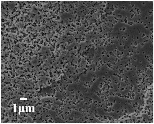
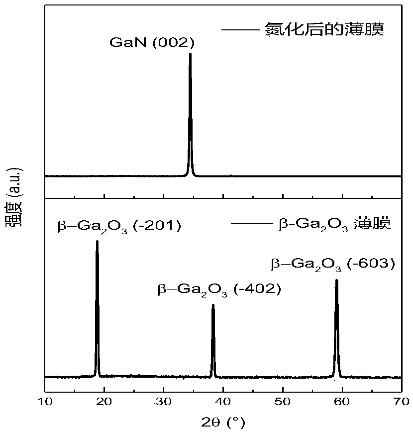
[0025] (1) Clean and treat the substrate sapphire, and use halide vapor phase epitaxy to grow uniformly distributed Ga on the sapphire substrate. 2 o 3For thin films, the reaction system mainly includes two temperature zones. In the low temperature zone, metal gallium reacts with HCl to generate GaCl as the gallium source, and the temperature is controlled at 850°C; oxygen is used as the oxygen source, and in the high temperature growth zone GaCl and O 2 Mix and react to obtain a gallium oxide film, and the temperature in the high temperature zone is 1000°C. The pressure is 1 atmosphere, O 2 / Ga input flow ratio is 3. By adjusting the growth time, gallium oxide films with different thicknesses can be obtained. Control Ga 2 o 3 Films were grown to a thickness of 3 µm, Ga 2 o 3 The thickness uniformity is above 90%.
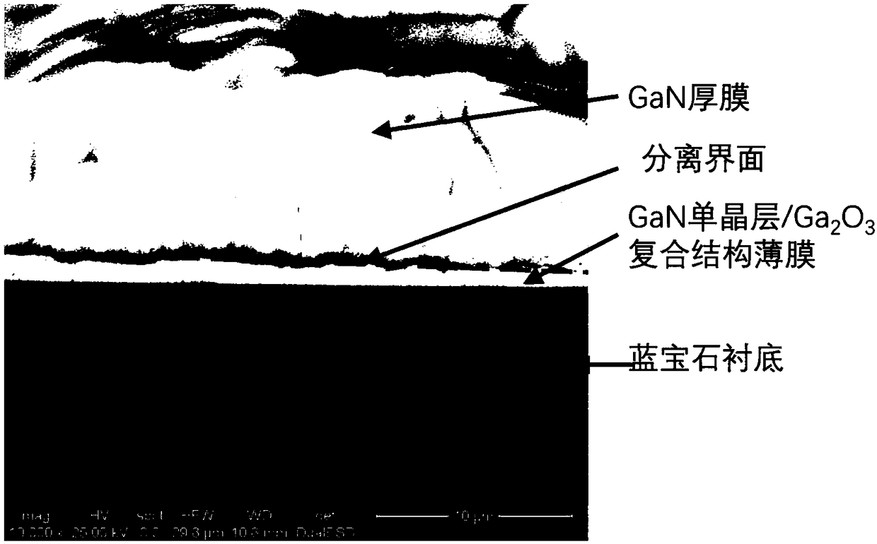
[0026] (2) Ga 2 o 3 The thin film substrate is placed in a high-tem...
Embodiment 2
[0030] The self-separation method for preparing GaN substrates, the steps include:
[0031] (1) Clean and treat the substrate sapphire, and use halide vapor phase epitaxy to grow uniformly distributed Ga on the sapphire substrate. 2 o 3 Thin films, the reaction system mainly includes two temperature zones, in the low temperature zone, metal gallium and Cl 2 The reaction generates GaCl as the gallium source at a temperature of 800°C; oxygen is used as the oxygen source, and in the high-temperature growth region GaCl and O 2 Mix and react to obtain a gallium oxide film, and the temperature in the high temperature zone is 800°C. The pressure is 1 atmosphere, O 2 The / Ga input flow ratio is 1.5. By adjusting the growth time, gallium oxide films with different thicknesses can be obtained. Control Ga 2 o 3 Films were grown to a thickness of 1 µm, Ga 2 o 3 The thickness uniformity is above 90%.
[0032] (2) Ga 2 o 3 The thin film substrate is placed in a high-temperature ...
Embodiment 3
[0036] The self-separation method for preparing GaN substrates, the steps include:
[0037] (1) Clean and treat the substrate sapphire, and use halide vapor phase epitaxy to grow uniformly distributed Ga on the sapphire substrate. 2 o 3 For thin films, the reaction system mainly includes two temperature zones. In the low temperature zone, metal gallium reacts with HCl to generate GaCl as the gallium source at a temperature of 900°C; oxygen is used as the oxygen source, and in the high temperature growth zone GaCl and O 2 Mix and react to obtain a gallium oxide film, and the temperature in the high temperature zone is 1050°C. The pressure is 1 atmosphere, O 2 The / Ga input flow ratio was 15. By adjusting the growth time, gallium oxide films with different thicknesses can be obtained. Control Ga 2 o 3 Films were grown to a thickness of 5 µm, Ga 2 o 3 The thickness uniformity is above 90%.
[0038] (2) Ga 2 o 3 The film substrate is placed in a high-temperature tube-ty...
PUM
| Property | Measurement | Unit |
|---|---|---|
| thickness | aaaaa | aaaaa |
| thickness | aaaaa | aaaaa |
| thickness | aaaaa | aaaaa |
Abstract
Description
Claims
Application Information