Preparation method for semiconductor material

A technology of semiconductor and chemical vapor deposition, which is applied in the direction of polycrystalline material growth, chemical instruments and methods, metal material coating technology, etc., can solve the problems of epitaxial growth difficulty, pollution, semiconductor material quality problems, etc., and achieve the improvement of surface chemical activity , avoid pollution, and facilitate the effect of epitaxial growth

Inactive Publication Date: 2019-02-05
SUZHOU INST OF NANO TECH & NANO BIONICS CHINESE ACEDEMY OF SCI
View PDF2 Cites 5 Cited by
  • Summary
  • Abstract
  • Description
  • Claims
  • Application Information

AI Technical Summary

Problems solved by technology

However, due to the lack of dangling bonds on the surface of graphene, direct epitaxial growth is difficult, and the grown semiconductor material has a large number of stacking faults, dislocations, etc., and the defect density is much higher than that of materials that can be applied to conventional devices.
On the other hand, the existing graphene is basically grown on the substrate supporting the metal catalyst. When used as a substrate, it needs to be separated from the metal catalyst and transferred out for use, but it will inevitably be polluted during the transfer process. , resulting in quality problems with semiconductor materials grown on it as a substrate

Method used


Image

  • Preparation method for semiconductor material
  • Preparation method for semiconductor material

Examples


preparation example Construction

[0017] An embodiment of the present invention provides a method for preparing a semiconductor material, including:

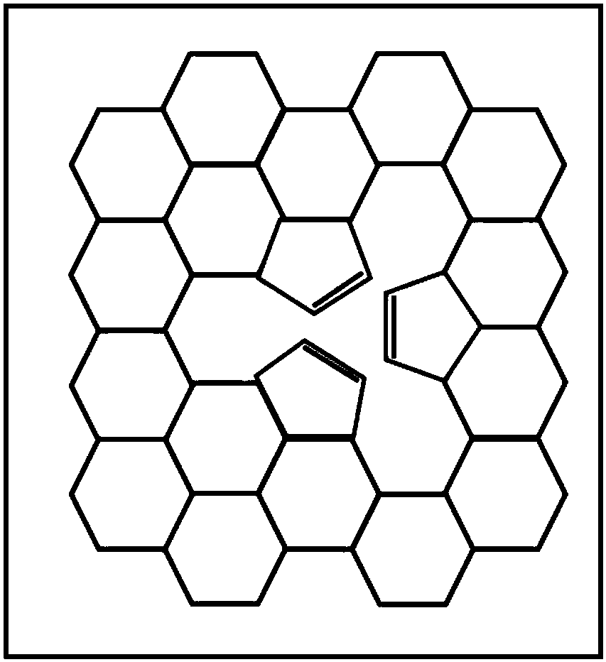
[0018] Graphene containing surface defects is grown by chemical vapor deposition on an unsupported metal catalyst substrate from ethylene and / or acetylene as a carbon source, and,

[0019] The graphene formed on the base and containing surface defects is used as a substrate, and the semiconductor material is epitaxially grown directly on the substrate.

[0020] Further, the semiconductor material includes GaN, AlN, InN, ZnO or SiC, but is not limited thereto.

[0021] Further, the reaction temperature used in the chemical vapor deposition method is 800-1200°C.

[0022] Further, the reaction atmosphere used in the chemical vapor deposition method includes any one or a combination of two or more of ethylene or acetylene, hydrogen, and argon, but is not limited thereto.

[0023] Preferably, the volume percentage of ethylene or acetylene in the reaction atmosphere...

Embodiment 1

[0036] Embodiment 1: take sapphire as substrate, ethylene is carbon source, utilize chemical vapor deposition method to grow graphene on substrate, specifically as follows:

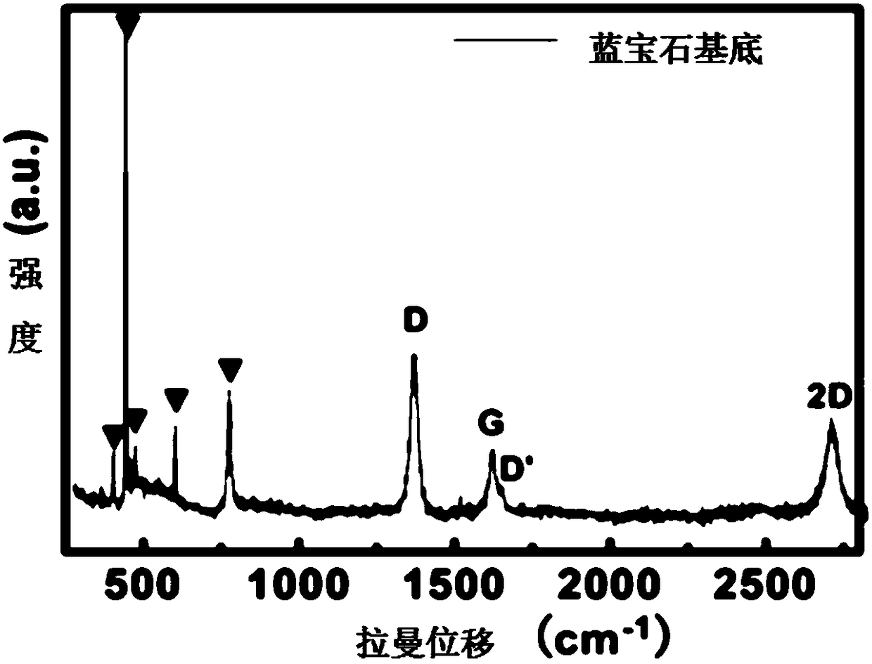
[0037] First, put the epitaxial sapphire substrate into the growth chamber, adjust the air pressure in the chamber to about 1Pa, remove the background oxygen, and then pass in argon gas of 900 sccm, and control the chamber air pressure to 5x10 by controlling the pumping speed of the dry pump. 4 Pa, raise the substrate temperature to 1200°C, keep it warm for about 10 minutes, and keep the chamber pressure constant during the process. Then pass 5sccm hydrogen gas for 2 minutes to clean the substrate surface, then pass 100sccm ethylene to grow graphene, and the growth time is 5 minutes; after the growth is completed, stop passing hydrogen and ethylene, quickly cool down to room temperature, and keep the argon gas unchanged. Keeping the pressure in the cavity constant, graphene with a large number of defects ...

Embodiment 2

[0045] Embodiment 2: take sapphire as substrate, and acetylene is carbon source, utilize chemical vapor deposition method to grow graphene on substrate, specifically as follows:

[0046] First put the epitaxial sapphire substrate into the growth chamber, adjust the air pressure in the chamber to 1Pa, remove the background oxygen, and then pass in argon gas 900sccm, and control the chamber air pressure to 5x10 by controlling the pumping speed of the dry pump. 4 Pa, raise the substrate temperature to 1000°C, keep it warm for about 10 minutes, keep the chamber pressure constant during this process, then pass 5 sccm hydrogen gas for 2 minutes to clean the substrate surface, and then pass 100 sccm acetylene to grow graphite Graphene, the growth time is 5 minutes; after the growth is completed, stop the flow of hydrogen and acetylene, quickly cool down to room temperature, keep the argon gas and the pressure in the chamber constant, and finally obtain graphene with a large number of ...


PUM


Abstract

The invention discloses a preparation method for semiconductor material The preparation method comprises the steps that ethylene and / or acetylene are / is adopted asa carbon source; a chemical vapour deposition method is adopted, and graphene containing surface defect grows on a substrate which metal catalyst is not loaded; and in addition, the grapheme which is formed on the substrate and containsthe surface defects is adopted as a substrate body, and a semiconducting material epitaxially grows on the substrate body directly. According to the preparation method for the semiconductor materials,the graphene containing the great number of defects can be directly prepared through the chemical vapour deposition method; chemical treatment is not needed to be additionally conducted on the surface of the graphene; surface chemistry activity of the graphene can be improved; the graphene which is large in size and is uniformly provided with the great number of defects is obtained; The obtainedgraphene is directly adopted as the substrate body to grow the semiconducting material; transfer is not needed; and the problem that contamination is introduced in the substrate transfer process, so that the growing semiconducting material has macroscopic defects is avoided.

Description

technical field [0001] The invention relates to a method for preparing a semiconductor material, in particular to a method for directly growing a semiconductor material with defective graphene as a substrate, and belongs to the technical field of semiconductor preparation technology. Background technique [0002] In 2004, British scientists discovered that the sp 2 Graphene, a new type of two-dimensional atomic crystal composed of hybrid-connected monoatomic layers, whose basic structural unit is the most stable six-membered benzene ring in organic materials, is currently the most ideal two-dimensional nanomaterial. Single-layer graphene refers to graphite with only one carbon atomic layer thickness, and C-C is connected by covalent bonds to form a honeycomb structure. In graphene, each carbon atom is connected to other 3 carbon atoms through a strong σ bond (the strongest chemical bond in nature). These strong C-C bonds make graphene sheets have excellent mechanical proper...

Claims


Application Information

Patent Timeline
Patent Type & Authority Applications(China)
IPC IPC(8): C23C16/30C23C16/02C30B25/18C30B29/10
CPCC01P2002/82C23C16/0272C23C16/30C30B25/183C30B29/10
Inventor 徐俞王建峰徐科
Owner SUZHOU INST OF NANO TECH & NANO BIONICS CHINESE ACEDEMY OF SCI
Why Eureka
Try Eureka