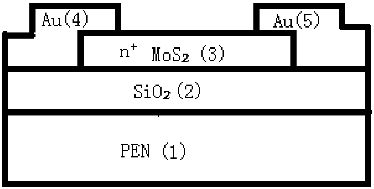
Flexible molybdenum disulfide phototransistor and preparation method thereof
A technology of phototransistor and molybdenum disulfide, which is applied in the direction of circuits, electrical components, semiconductor devices, etc., can solve the problems of complex steps of flexible phototransistor methods, high manufacturing costs of flexible phototransistors, and inapplicability of flexible transistors, and achieve the difficulty of manufacturing process Low, improved photoelectric performance, narrow bandgap effect
- Summary
- Abstract
- Description
- Claims
- Application Information
AI Technical Summary
Problems solved by technology
Method used
Image

Examples
Embodiment 1
[0033] Example 1, preparing a flexible molybdenum disulfide phototransistor with a molybdenum disulfide film thickness of 5.2 nm.
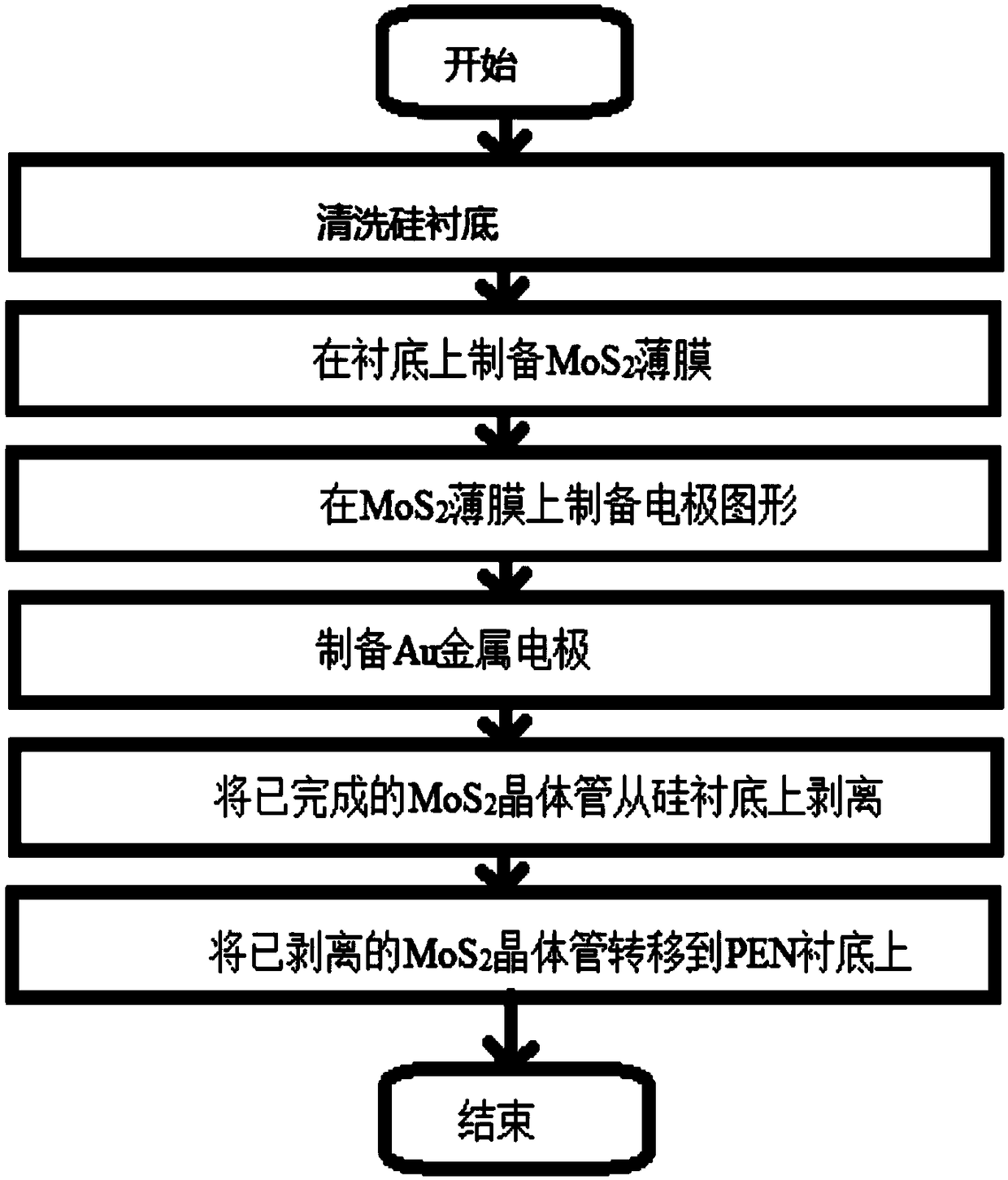
[0034] Step 1: Clean the silicon substrate.
[0035] will have a 280nm thick SiO 2 The p-type heavily doped silicon wafers were ultrasonically cleaned in acetone and isopropanol for 15 minutes to remove surface pollutants, and dried with a nitrogen gun after cleaning.
[0036] Step 2: Preparation of MoS on the cleaned substrate 2 film.
[0037] The 5.2nm thick MoS was first coated with scotch tape 2 Thin films from MoS 2 peel off on solid;
[0038] MoS 2 The tape of the film is tightly attached to the silicon substrate that has been cleaned in step 1;
[0039] Then tear off the scotch tape to make the MoS 2 A thin film remains on the silicon wafer.
[0040] Step 3: In MoS 2 Electrode patterns are prepared on the film.
[0041] 3a) With MoS 2 Spin-coat MICROPOSIT S1811 photoresist with a thickness of 4 μm on the silicon wafer of the fil...
Embodiment 2
[0055] Example 2, preparing a flexible molybdenum disulfide phototransistor with a molybdenum disulfide film thickness of 1 nm.
[0056] Step 1, cleaning the silicon substrate.
[0057] will have a 200nm thick SiO 2 The p-type heavily doped silicon wafers were ultrasonically cleaned in acetone and isopropanol for 15 minutes to remove surface pollutants, and dried with a nitrogen gun after cleaning.
[0058] Step 2: Prepare MoS on the cleaned substrate 2 film.
[0059] First use scotch tape to cover the 1nm thick MoS 2 Thin films from MoS 2 The solid was peeled off; then the sticky MoS 2 The tape of the film is tightly attached to the silicon substrate that has been cleaned in step 1; then the scotch tape is torn off to make the MoS 2 A thin film remains on the silicon wafer.
[0060] Step 3: In MoS 2 Electrode patterns are prepared on the film.
[0061] First, with MoS 2 Spin-coat MICROPOSIT S1811 photoresist with a thickness of 3 μm on the silicon wafer of the film,...
Embodiment 3
[0072] Example 3, preparing a flexible molybdenum disulfide phototransistor with a molybdenum disulfide film thickness of 6 nm.
[0073] Step A, cleaning the silicon substrate.
[0074] Will be with 300nm thick SiO 2 The p-type heavily doped silicon wafers were ultrasonically cleaned in acetone and isopropanol for 15 minutes to remove surface pollutants, and dried with a nitrogen gun after cleaning.
[0075] Step B: Preparation of MoS on the cleaned substrate 2 film.
[0076] B1) Use scotch tape to cover the 6nm thick MoS 2 Thin films from MoS 2 peel off on solid;
[0077] B2) will stick MoS 2 The adhesive tape of the film is tightly attached to the silicon substrate that has been cleaned in step A, and then the scotch tape is torn off to make the MoS 2 A thin film remains on the silicon wafer.
[0078] Step C: In MoS 2 Electrode patterns are prepared on the film.
[0079] C1) with MoS 2 Spin-coat MICROPOSIT S1811 photoresist with a thickness of 5 μm on the silicon ...
PUM
 Abstract
Description
Claims
Application Information