Single-photon avalanche diode, manufacturing method thereof, detector array and image sensor

A single-photon avalanche and diode technology, applied in diodes, electro-solid devices, semiconductor devices, etc., can solve the problems of reduced absorption efficiency of incident photons, reduced absorption efficiency, and difficult processing of excessively thick device layers, so as to improve light absorption efficiency. , Improve the absorption efficiency and overcome the effect of low light absorption efficiency

Pending Publication Date: 2019-04-19
SHENZHEN ADAPS PHOTONICS TECH CO LTD
View PDF0 Cites 16 Cited by
  • Summary
  • Abstract
  • Description
  • Claims
  • Application Information

AI Technical Summary

Problems solved by technology

However, an overly thick device layer requires a corresponding increase in the area of ​​the SPAD, which reduces the number of units per unit area, and the processing of an overly thick device layer is difficult, the yield is low, and it is not easy to be compatible with the CMOS process, which increases the cost.
Additionally, using thick silicon increases the jitter time of the SPAD, and greater jitter time reduces the accuracy of range detection in LiDAR or other time-of-flight based applications
[0010] (2) Increase the incident rate of light by adding an anti-reflection film on the surface of the planar structure of the SPAD, but its anti-reflection effect will decrease with the increase of the incident angle, resulting in a decrease in the absorption efficiency

Method used


Image

  • Single-photon avalanche diode, manufacturing method thereof, detector array and image sensor
  • Single-photon avalanche diode, manufacturing method thereof, detector array and image sensor
  • Single-photon avalanche diode, manufacturing method thereof, detector array and image sensor

Examples


Embodiment 1

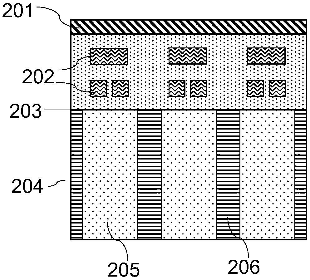
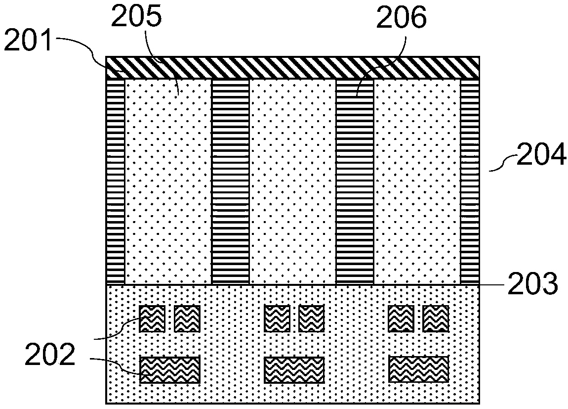
[0068] A back-illuminated single-photon avalanche diode. The back-illuminated single-photon avalanche diode is sequentially provided with a substrate, a circuit layer, a silicon oxide layer, and a silicon detection layer from bottom to top. The silicon detection layer includes a first-type doped region, a second Type doped region, third type doped region and side wall reflection wall, the second type doped region or the third type doped region forms a multiplication junction with the first type doped region, the third type doped region is In the doping region where the doping concentration changes, a light trapping structure is arranged in the back-illuminated single photon avalanche diode. Further, an anti-reflection structure is also provided on the upper surface of the back-illuminated single photon avalanche diode.

[0069] Since the back-illuminated single-photon avalanche diode is equipped with a light-trapping structure and a side wall reflective wall, the incident ligh...

Embodiment 2

[0071] Embodiment 2 is obtained based on the further improvement of Embodiment 1. The light trapping structure is arranged on the upper surface of the back-illuminated single photon avalanche diode and / or above and / or below the silicon oxide layer, and the light trapping structure on the upper surface The light-trapping structure above the silicon oxide layer or the light-trapping structure below the silicon oxide layer can be set alone to improve the light absorption efficiency of the back-illuminated SPAD, and can also be used in combination. Further, the light-trapping structure is a nanoscale or micron-scale concave-convex structure, for example, the light-trapping structure can be an inverted pyramid structure 1 (refer to Figure 10 ) or shallow trench structure 20 (such as Figure 12 As shown, the shallow trench structure 20 is arranged on the upper surface of the SPAD), or the surface is a structure such as a honeycomb surface, a sinusoidal grating textured surface, a d...

Embodiment 3

[0075] Obtain embodiment 3 based on the further improvement of embodiment 1, refer to Figure 10 , Figure 10 It is a schematic cross-sectional structure diagram of the third embodiment of a back-illuminated single-photon avalanche diode in the present invention; the light-trapping structure and / or the anti-reflection structure is an inverted pyramid structure 1, and the inverted pyramid structure 1 has both light-trapping and anti-reflection functions Specifically, the inverted pyramid structure 1 is disposed on the upper surface of the back-illuminated SPAD (that is, disposed above the third-type doped region 8), and the inverted pyramid structure 1 is obtained by filling silicon oxide after etching on the silicon base. In this embodiment, an insulating dielectric protection layer 13 is provided above the inverted pyramid structure 1 for protecting the SPAD. Specifically, the inverted pyramid structure 1 placed on the upper surface of the SPAD can form a gentle and gradual ...


PUM


Abstract

The invention discloses a single photon avalanche diode, a manufacturing method thereof, a detector array, and an image sensor. The back-illuminated single-photon avalanche diode is provided with a light trapping structure and a side wall reflecting wall. Incident light is scattered to all angles after being reflected, scattered and refracted by the light trapping structure, and the effective optical path of the light in the back-illuminated single-photon avalanche diode can be prolonged under the reflection action of the side wall reflection wall, so that the absorption efficiency of the light in the back-illuminated single-photon avalanche diode is improved. The invention relates to the manufacturing method of the back-illuminated single-photon avalanche diode, which realizes the manufacturing of the back-illuminated single-photon avalanche diode. Due to the fact that the photoelectric detector array and the image sensor comprise the back-illuminated single-photon avalanche diode, the light absorption efficiency of the photoelectric detector array and the image sensor is effectively improved.

Description

technical field [0001] The invention relates to the field of optoelectronics, in particular to a single-photon avalanche diode, a manufacturing method, a detector array, and an image sensor. Background technique [0002] Image sensors are widely used in various electronic devices, such as digital cameras, mobile phones, medical imaging equipment, security inspection equipment, distance measuring cameras and so on. With the continuous improvement of semiconductor technology for manufacturing image sensors, image sensors are further developing in the direction of low power consumption, miniaturization, and high integration. Image sensors typically consist of an array of photodetectors. A single photon avalanche diode (SPAD) is a type of photodetector that can be used in an image sensor. [0003] Single Photon Avalanche Diodes (SPADs) can be used in a variety of industrial and academic applications, depth detection (including lidar), medical sensing, machine vision, gesture r...

Claims


Application Information

Patent Timeline
IPC IPC(8): H01L31/0232H01L31/107H01L27/144H01L27/146H01L31/18
CPCH01L27/1443H01L27/1446H01L27/1464H01L31/02327H01L31/107H01L31/1804H01L27/1463H01L27/14634H01L27/14629H01L27/1469H01L27/14627H01L27/14643H01L27/14685H01L31/02027
Inventor 臧凯李爽马志洁
Owner SHENZHEN ADAPS PHOTONICS TECH CO LTD
Why Eureka
Try Eureka