A Digital Impedance Adaptive Laser Diode Driver
A laser diode, self-adaptive technology, applied in the direction of lasers, laser components, semiconductor lasers, etc., can solve the problems of no over-current power-off and over-temperature power-off protection functions, laser diode damage, etc.
- Summary
- Abstract
- Description
- Claims
- Application Information
AI Technical Summary
Problems solved by technology
Method used
Image
Examples
Embodiment 1
[0040] Embodiment 1 Overall structure of the present invention
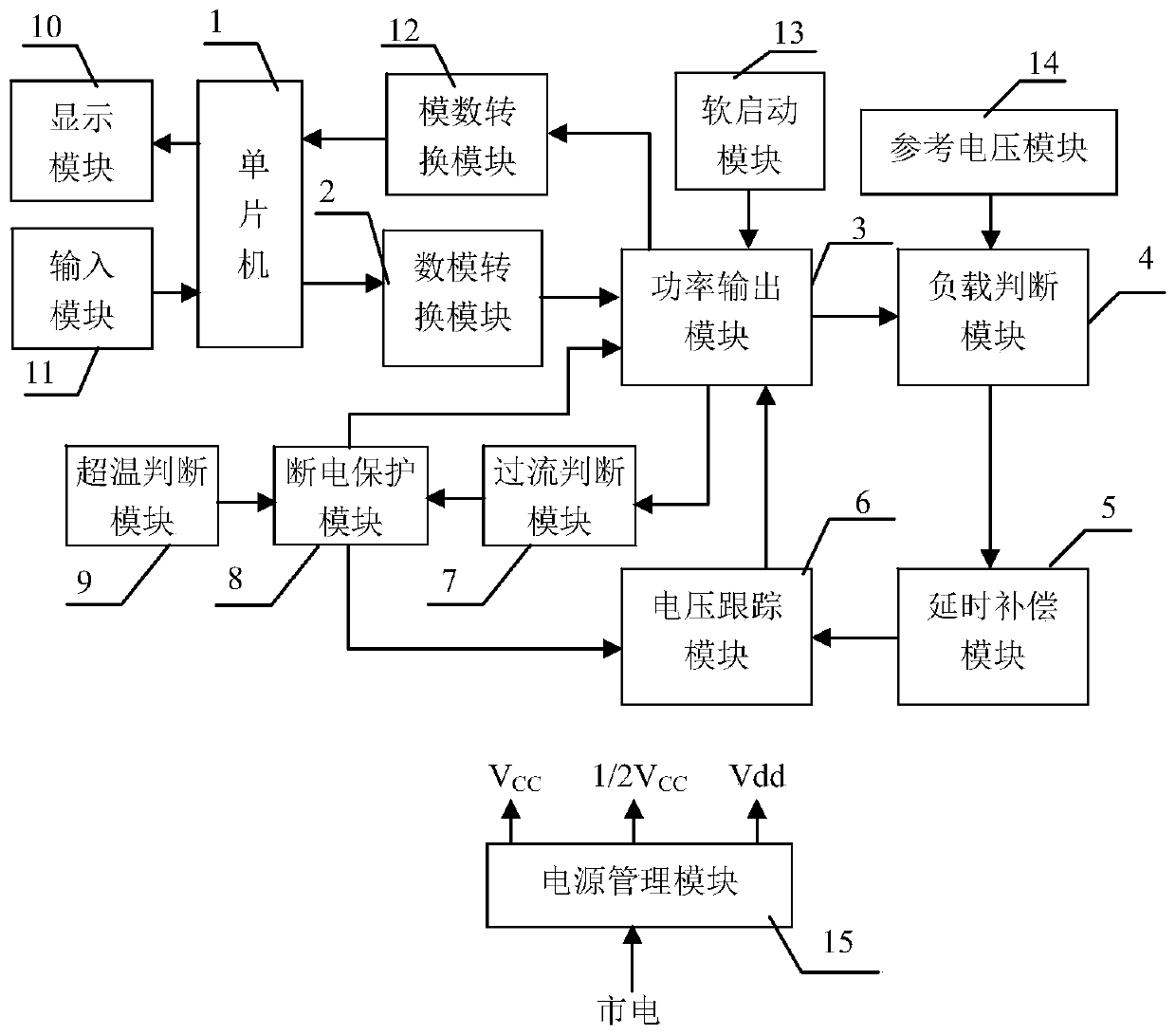
[0041] Overall structure of the present invention is as figure 1 As shown, there are single-chip microcomputer 1, digital-to-analog conversion module 2, power output module 3, load judgment module 4, delay compensation module 5, voltage tracking module 6, over-current judgment module 7, power-off protection module 8, over-temperature judgment module 9 display module 10, input module 11, analog-to-digital conversion module 12, soft-start module 13, reference voltage module 14, power management module 15; wherein, single-chip microcomputer 1 is respectively connected with display module 10, input module 11, analog-to-digital conversion module 12, The digital-to-analog conversion module 2 is connected, the digital-to-analog conversion module 2 is connected to the power output module 3, the soft start module 13 is connected to the power output module 3, and the power output module 3 is connected to the analog-to-digi...
Embodiment 2
[0042] Embodiment 2 The power output module of the present invention
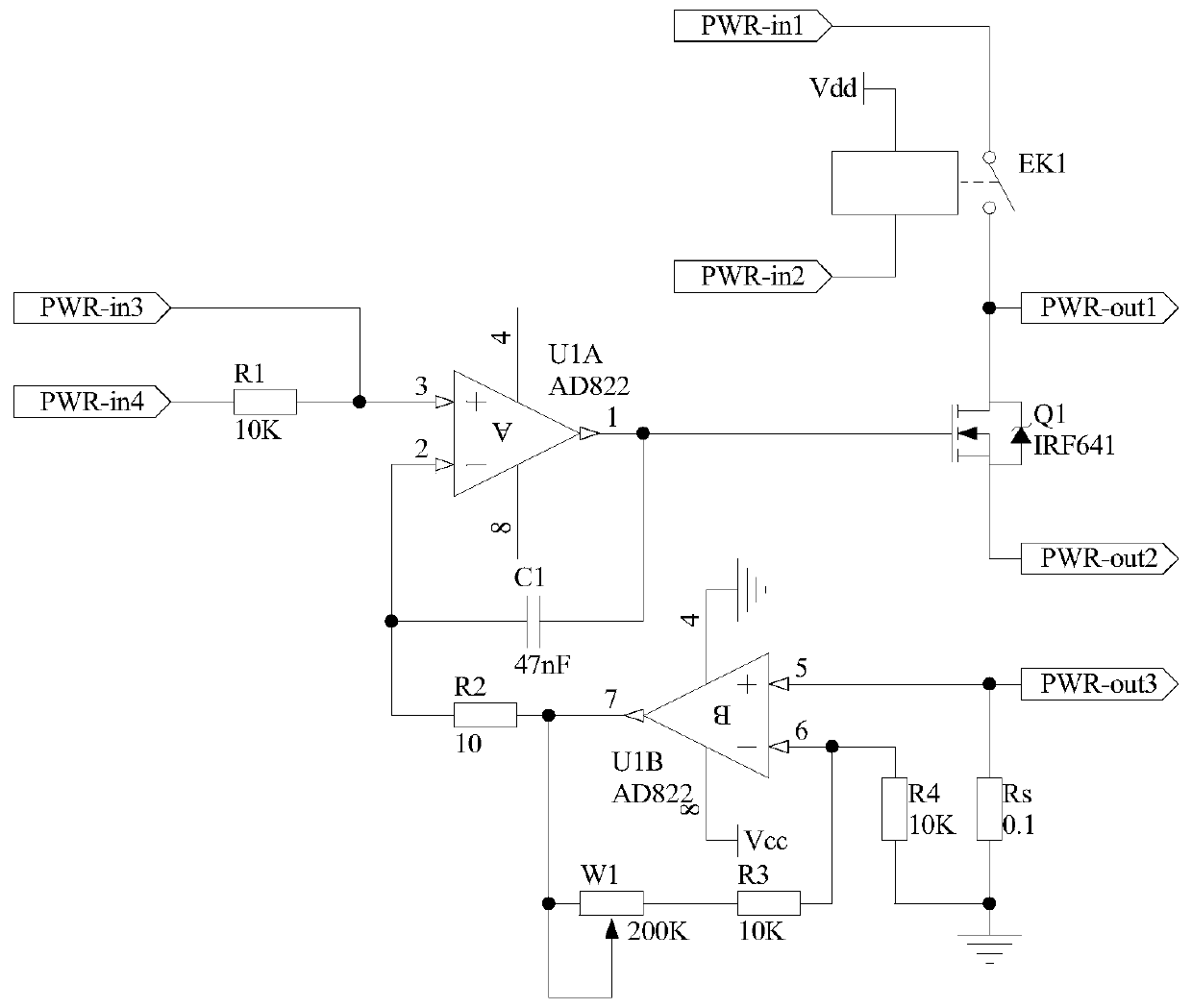
[0043] The schematic circuit diagram of the power output module 3 is as follows image 3 As shown, one end of the switch of the relay EK1 is used as the first input end of the power output module 3, which is marked as port PWR-in1, and the other end is connected to the drain of the field effect transistor Q1, and is used as the first output end of the power output module 3 terminal, denoted as port PWR-out1, one end of the coil of relay EK1 is connected to the power supply Vdd, and the other end is used as the second input terminal of power output module 3, denoted as port PWR-in2, the gate of FET Q1 is connected to the operational amplifier The output terminal of U1A is connected, and the source is used as the second output terminal of the power output module 3, which is recorded as port PWR-out2. The input end is marked as port PWR-in3, and the other end of resistor R1 is used as the fourth input end of ...
Embodiment 3
[0045] Embodiment 3 The load judging module of the present invention
[0046] The principle circuit of the load judging module 4 is as Figure 4As shown, the non-inverting input terminal of the operational amplifier U2A is used as the first input terminal of the load judgment module 4, which is denoted as port Vjdg-in1, and is connected to the port PWR-out1 of the power output module 3, and the inverting input terminal of the operational amplifier U2A is connected to the The output terminal of operational amplifier U2A is connected to one end of resistor R5, the other end of resistor R5 is connected to one end of resistor R6 and the same-inverting input terminal of operational amplifier U3A, the other end of resistor R6 is grounded, and the output terminal of operational amplifier U3A is connected to the in-phase input terminal of operational amplifier U3A. One end is connected to one end of the resistor R9, the other end of the resistor R8 is connected to the inverting input ...
PUM
 Abstract
Description
Claims
Application Information


