An ultrasonic-assisted microstructure selective forming manufacturing device and method based on digital light

An ultrasonic-assisted, device-manufacturing technology, applied in microstructure devices, manufacturing microstructure devices, microstructure technology, etc., can solve the problems of lack of control methods and devices for three-dimensional microstructure forming areas, and achieve fast response speed and high control accuracy Effect

Active Publication Date: 2019-05-10
ZHEJIANG UNIV
View PDF9 Cites 3 Cited by
  • Summary
  • Abstract
  • Description
  • Claims
  • Application Information

AI Technical Summary

Problems solved by technology

In summary, there is a lack of a method and device for controlling the three-dimensional microstructure forming area in the prior art

Method used


Image

  • An ultrasonic-assisted microstructure selective forming manufacturing device and method based on digital light
  • An ultrasonic-assisted microstructure selective forming manufacturing device and method based on digital light
  • An ultrasonic-assisted microstructure selective forming manufacturing device and method based on digital light

Examples


Embodiment 1

[0049] Such as Figure 4 As shown, this embodiment is a schematic diagram of the implementation results of turning on two pairs of transducers and using a hexagonal digital mask.

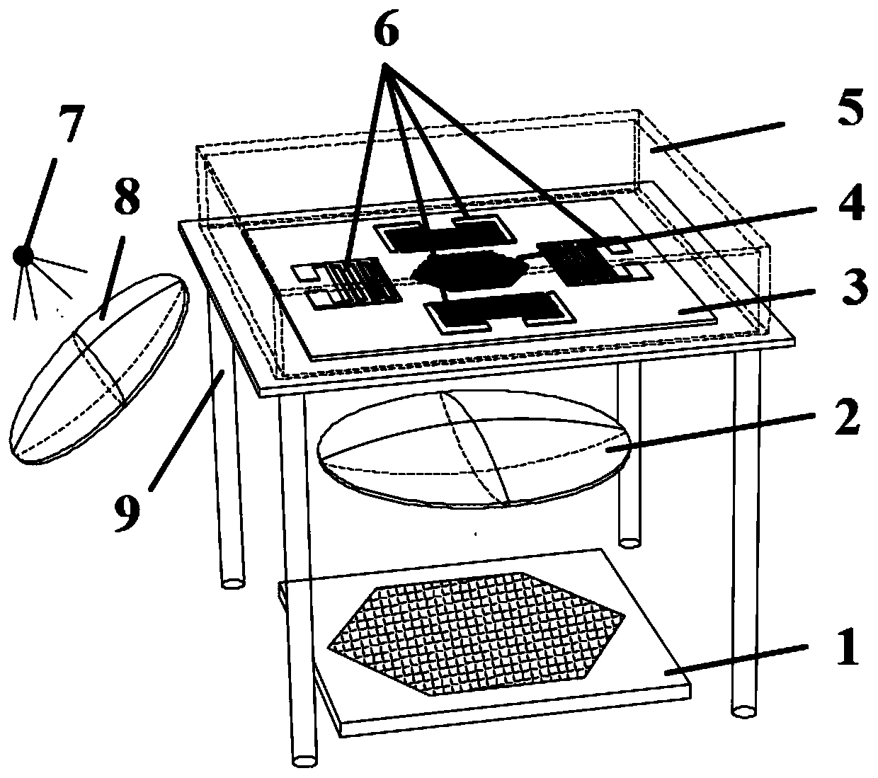
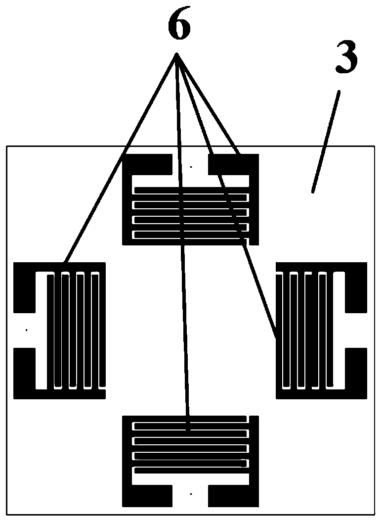
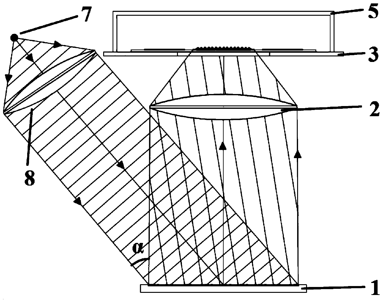
[0050] Step 1) Apply a photosensitive liquid 4 on the double-sided polished lithium niobate wafer 3 with a micropipette, so that the photosensitive liquid 4 evenly covers the central area of ​​the double-sided polished lithium niobate wafer 3, and convert the two pairs of fingers The signal generator is connected with the signal generator, the signal generator is started, and the interdigital transducer 6 uses the inverse piezoelectric effect to generate a stable acoustic surface standing wave field on the double-sided polished lithium niobate wafer 3, and the acoustic surface standing wave field is coupled into the photosensitive In the liquid 4, the photosensitive liquid 4 is subjected to the acoustic radiation force in the two-dimensional acoustic surface standing wave field to generate periodic ...

Embodiment 2

[0055] Such as Figure 5 As shown, this embodiment is a schematic diagram of the implementation result of turning on a pair of transducers and using an arrayed circular digital mask.

[0056] Step 1) Coating the photosensitive liquid 4 on the double-sided polished lithium niobate wafer 3 with a micropipette, so that the photosensitive liquid 4 evenly covers the central area of ​​the double-sided polished lithium niobate wafer 3, and transducing a pair of fingers The signal generator is connected to the signal generator, the signal generator is started, and the interdigital transducer 6 uses the inverse piezoelectric effect to generate the acoustic surface standing wave field on the double-sided polished lithium niobate wafer 3, and the acoustic surface standing wave field is coupled into the photosensitive liquid In 4 , the photosensitive liquid 4 is subjected to the acoustic radiation force in the acoustic surface standing wave field to generate periodic microstructure patter...

Embodiment 3

[0060] Such as Image 6 As shown, this embodiment is a schematic diagram of the implementation results of turning on two pairs of transducers, using an arrayed circular digital reticle and a square digital reticle at the same time, and combining the secondary exposure.

[0061] Step 1) Coating a photosensitive liquid 4 on the double-sided polished lithium niobate wafer 3, connecting two pairs of interdigital transducers to the signal generator, starting the signal generator, and the interdigital transducer 6 is polished on both sides of the niobate The acoustic surface standing wave field generated on the lithium wafer 3 is coupled into the photosensitive liquid 4 , thereby forming a corrugated microstructure array on the surface of the photosensitive liquid 4 .

[0062] Step 2) Place the PDMS nitrogen protective shell 5 above the two pairs of interdigital transducers 6, and pass nitrogen gas into the PDMS nitrogen protective shell 5 to exhaust the air. After the microstructur...


PUM


Abstract

The invention discloses an ultrasonic-assisted microstructure selective forming manufacturing device and method based on digital light. The double-sided polishing lithium niobate wafer is arranged onthe light transmission hole of the optical bracket; the at least one pair of interdigital transducers are orthogonally arranged around the wafer, the PDMS nitrogen protection shell is arranged above the transducers, the converging lens and the digital microprism chip are sequentially arranged under the light transmission hole, and the ultraviolet light source and the collimating lens are sequentially and obliquely arranged on the side surface of the optical bracket. The wafer is coated with photosensitive liquid, and the interdigital transducer is started to enable the standing wave field of the acoustic surface to be coupled into the photosensitive liquid to form a microstructure array; a nitrogen protection shell is placed, the nitrogen protection shell is input into a DMD mask, ultraviolet light is irradiated on the digital microprism chip for selective reflection after passing through the collimating lens, then sequentially penetrating through the converging lens and the wafer to be irradiated into the photosensitive liquid, and the photosensitive liquid in an exposure area is cured to obtain the microstructure array film in a specified shape. Digital selection of ultraviolet light is achieved, the control precision of a forming area is high, and the response speed is high.

Description

technical field [0001] The invention relates to rapid prototyping technology, in particular to a digital light-based ultrasonic-assisted microstructure selective forming manufacturing device and method. Background technique [0002] Common fabrication methods of polymer surface microstructures include 3D printing, photolithography, nanoimprinting, ultrasonic standing wave field assistance, etc. Among them, the array microstructure forming method based on the ultrasonic standing wave field has the advantages of fast forming speed, no need for molds in the forming process, and multi-material manufacturing. It can be applied to cell chip substrates, flexible micro-electrodes, and distributed flexible tactile sensors. In the fabrication of microstructures with polymer substrates. For example, the one-dimensional or two-dimensional array microstructures assisted by ultrasonic standing wave field can be used as the base material of cell chips for the study of three-dimensional cu...

Claims


Application Information

Patent Timeline
Patent Type & Authority Applications(China)
IPC IPC(8): B81C1/00B82Y40/00
Inventor 汪延成韩晨阳梅德庆许诚瑶
Owner ZHEJIANG UNIV
Why Eureka
Try Eureka