Totally-inorganic LED packaging method and packaging structure

A technology for LED packaging and LED chips, applied in electrical components, circuits, semiconductor devices, etc., can solve problems such as increasing the risk of device failure, product failure, and decline in UV resistance, improving UV aging resistance, and simplifying the production process. , the effect of reducing the risk of failure

Inactive Publication Date: 2019-05-10
湖北深紫科技有限公司
View PDF9 Cites 7 Cited by
  • Summary
  • Abstract
  • Description
  • Claims
  • Application Information

AI Technical Summary

Problems solved by technology

However, organic materials will cause yellowing and cracking under ultraviolet radiation, reducing the service life of LEDs
Especially for UV LEDs that emit light below 365nm, because as the wavelength band becomes shorter and the radiation energy becomes stronger, the UV resistance of organic resin materials will drop sharply, which will inevitably affect the life and stability of UV LEDs
In addition to UV aging, in terms of thermodynamics, there must be two interface substances, organic an

Method used


Image

  • Totally-inorganic LED packaging method and packaging structure
  • Totally-inorganic LED packaging method and packaging structure
  • Totally-inorganic LED packaging method and packaging structure

Examples


Embodiment 1

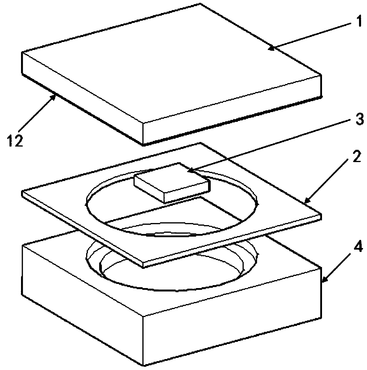
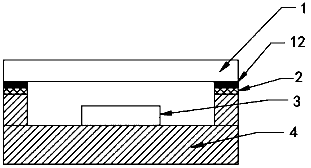
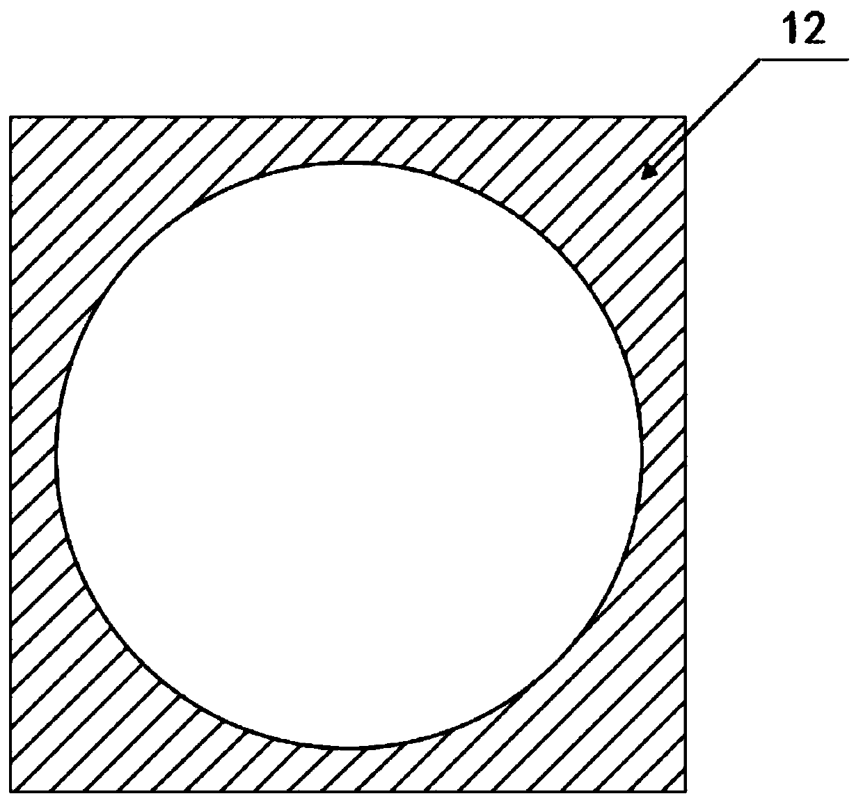
[0028] Such as Figure 1-Figure 3 As shown, the embodiment of the present invention provides an all-inorganic LED packaging structure, including a quartz light window 1 with a metallized frame, silver-copper nano paste 2, an LED chip 3 and a metal dam bracket 4, and the LED chip 3 is located on the metal dam In the center of the support 4, the metallized frame quartz light window 1 is located on the metal dam support 4, and the metal dam support 4 passes through the silver-copper nano paste 2 and the metallized frame quartz light window Phase 1 welding: the upper surface of the metal dam support 4 is a plane as the welding surface with the metallized frame quartz light window, and the silver-copper nano-paste 2 is provided on the welding surface of the metal dam support The metallized frame 21 on the bottom surface of the metallized frame quartz light window 1 matches the pattern of the welded surface of the metal dam support 4 .

[0029] The packaging method of the above-men...

Embodiment 2

[0042] Such as Figure 1-Figure 3 As shown, the embodiment of the present invention provides an all-inorganic LED packaging structure whose structural features are the same as those in Embodiment 1. The difference is that the preparation method is different:

[0043] The packaging method of the all-inorganic LED packaging structure provided by the embodiment of the present invention includes LED chip solidification, plasma cleaning, spot coating of silver-copper nano-paste, preparation of metallized frame quartz light window, low-temperature sintering and curing and other process steps (compared with the embodiment 1 is in the step 3 part), as follows:

[0044] Step 1. LED chip solidification: In LED chip solidification, use a solid crystal machine to place the LED chip inside the cleaned metal dam bracket. The solid crystal material can use silver glue, metal solder paste and gold-tin co- For crystal packaging, the heat resistance temperature is required to be not less than...

Embodiment 3

[0056] Such as Figure 1-Figure 3 As shown, the embodiment of the present invention provides an all-inorganic LED packaging structure. The structural features are the same as those in Embodiment 1, except that the preparation method is different:

[0057] The packaging method of the all-inorganic LED packaging structure provided by the embodiment of the present invention includes LED chip solidification, plasma cleaning, spot coating of silver-copper nano-paste, preparation of metallized frame quartz light window, low-temperature sintering and curing and other process steps (compared with the embodiment 1 is in the step 3 part), as follows:

[0058] Step 1. LED chip solidification: In LED chip solidification, use a solid crystal machine to place the LED chip inside the cleaned metal dam bracket. The solid crystal material can use silver glue, metal solder paste and gold-tin co- For crystal packaging, the heat resistance temperature is required to be not less than 200°C;

[0...


PUM

PropertyMeasurementUnit
Heat resistance temperatureaaaaaaaaaa
Thicknessaaaaaaaaaa
Thicknessaaaaaaaaaa

Abstract

The invention provides a totally-inorganic LED packaging method. The method includes following steps: placing an LED chip in a cleaned metal dam support by employing a die bonder; performing plasma cleaning after die bonding; dispensing silver-copper nanometer paste: uniformly dispensing the silver-copper nanometer paste on a welding surface of the metal dam support by employing the dispenser; preparing a metallized frame quartz optical window; and performing low-temperature sintering curing: covering the welding surface of the metal dam support by the metallized frame quartz optical window prepared in step 4 by employing the die bonder, and performing low-temperature sintering curing in a nitrogen atmosphere or a vacuum atmosphere. The invention also provides a totally-inorganic LED packaging structure prepared by the method. According to the method and the structure, the metallized frame quartz window and the metallized support are connected through the silver-copper nanometer paste,the usage of organic glue is avoided, the ultraviolet aging resistance of the packaging structure is improved, the failure risk is reduced, the process is simple, the usage is convenient, and the method and the structure can be applicable to mass production.

Description

technical field [0001] The invention relates to the technical field of LED packaging, in particular to an all-inorganic LED packaging method and packaging structure. Background technique [0002] At present, common LED packaging methods use organic materials such as resins for packaging to varying degrees. However, organic materials will cause yellowing and cracking under ultraviolet radiation, which will reduce the service life of LEDs. Especially for UV LEDs that emit light below 365nm, because as the wavelength band becomes shorter and the radiation energy becomes stronger, the UV resistance of organic resin materials will drop sharply, which will inevitably affect the life and stability of UV LEDs. In addition to UV aging, in terms of thermodynamics, there must be two interface substances, organic and inorganic, in the traditional visible light packaging method, and the thermal expansion coefficient of inorganic substances is much smaller than that of organic substances...

Claims


Application Information

Patent Timeline
IPC IPC(8): H01L33/56H01L33/62H01L33/48
Inventor 梁仁瓅许琳琳张爽张会雪葛鹏戴江南陈长清
Owner 湖北深紫科技有限公司
Why Eureka
Try Eureka