A method for processing top-contact organic field-effect transistors by laser

A technology of laser processing and contact structure, which is applied in the manufacture of semiconductor devices, electrical solid-state devices, semiconductor/solid-state devices, etc. It can solve the problems of device resolution and performance degradation, device processing quality is difficult to guarantee, and graphene pattern resolution is low. , to achieve high production efficiency, realize large-scale manufacturing and large-scale industrialization, and achieve the effect of small contact resistance

Active Publication Date: 2019-08-27
GUANGDONG UNIV OF TECH
View PDF1 Cites 0 Cited by
  • Summary
  • Abstract
  • Description
  • Claims
  • Application Information

AI Technical Summary

Problems solved by technology

However, this method greatly increases the complexity of manufacturing and low production efficiency; and the resolution of graphene patterns produced by chemical vapor deposition is low, which leads to a significant decrease in the resolution and performance of the entire device
[0008] To sum up, in the current manufacturing process of organic field effect transistors with top contact structure, there are still problems such as complex electrode processing technology and difficult to guarantee the quality of device processing. It is urgent to provide a high-quality processing method for organic field effect transistors with top contact structure.

Method used


Image

  • A method for processing top-contact organic field-effect transistors by laser
  • A method for processing top-contact organic field-effect transistors by laser
  • A method for processing top-contact organic field-effect transistors by laser

Examples


Embodiment 1

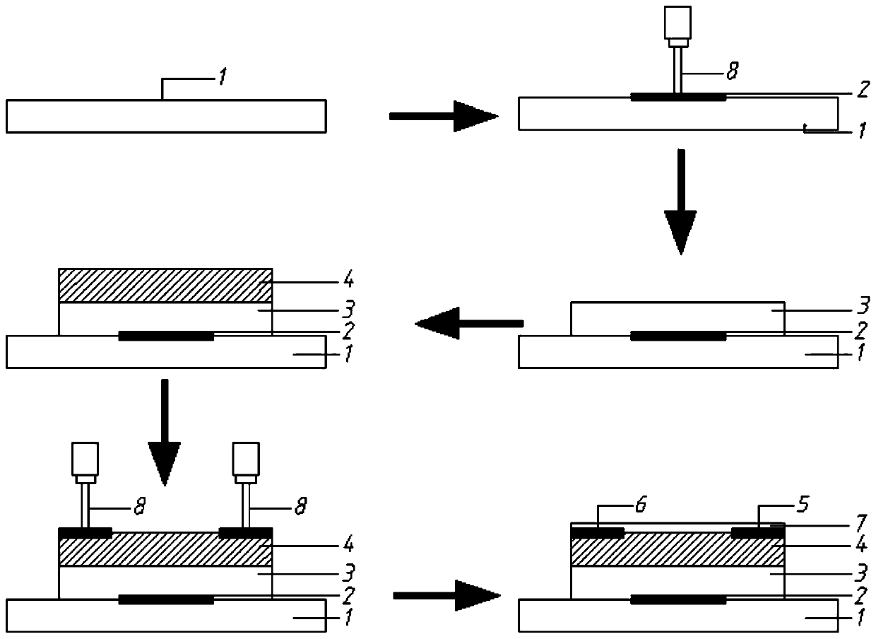
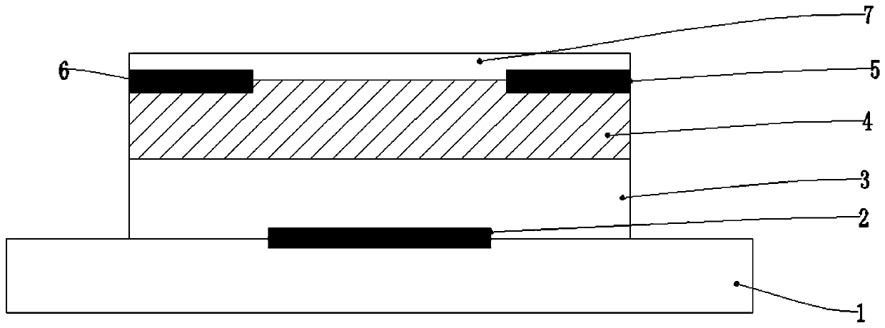
[0053] The method for processing an organic field-effect transistor with a top-contact structure by laser in this embodiment is used to prepare an organic field-effect transistor with a bottom-gate top-contact structure, such as figure 1 shown, including the following steps:

[0054] Step A, use cleaning powder to scrub the flexible substrate 1 with a thickness of 120 μm, then divide the flexible substrate 1 into 3 cm×2 cm, then ultrasonically clean it with acetone, ethanol and deionized water, and then dry it with nitrogen, And through surface plasma treatment, the surface of the flexible substrate 1 becomes hydrophilic;

[0055] Step B, the parameters of the laser processing system 8 are set as the processing parameters of the gate electrode 2 and the processing pattern is set as the pattern of the gate electrode 2, and then the laser processing system 8 performs laser processing on the area where the gate electrode 2 is set on the flexible substrate 1 , converting the surf...

Embodiment 2

[0095] The preparation scheme of the bottom gate top contact structure organic field effect transistor of the present embodiment is as follows:

[0096] Step 1, such as figure 1 As shown, a polyimide film with a thickness of 120 μm was selected as the flexible substrate 1, and the flexible substrate 1 was scrubbed with detergent powder, and then the flexible substrate 1 was divided into 3 cm × 2 cm, and then cleaned with acetone and ethanol respectively. Ultrasonic cleaning with deionized water, then drying with nitrogen, and surface plasma treatment, so that the surface of the flexible substrate 1 becomes hydrophilic;

[0097] Step 2, the parameters of the laser processing system 8 are set as the processing parameters of the grid electrode 2 and the processing pattern is set as the pattern of the grid electrode 2, the processing parameters of the grid electrode 2 are: the power duty cycle is 40% and the laser scanning speed is 100mm / s, the pattern size of the gate electrode ...

Embodiment 3

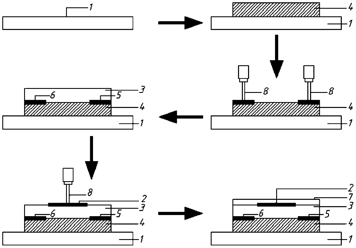
[0110] The preparation scheme of the top gate top contact structure organic field effect transistor of this embodiment is as follows:

[0111] Step 1, such as image 3 As shown, a polyimide film with a thickness of 120 μm was selected as the flexible substrate 1, and the flexible substrate 1 was scrubbed with detergent powder, and then the flexible substrate 1 was divided into 3 cm × 2 cm, and then cleaned with acetone and ethanol respectively. Ultrasonic cleaning with deionized water, then drying with nitrogen, and surface plasma treatment, so that the surface of the flexible substrate 1 becomes hydrophilic;

[0112] Step 2, mixing poly-3-hexylthiophene and absolute ethanol at a volume ratio of 5:1, and stirring in a magnetic stirrer for 10 minutes to obtain an organic semiconductor solution;

[0113] Step 3, put the flexible substrate 1 on the workbench of the glue homogenizer, take 3 drops of the organic semiconductor solution in step 2 with a pipette and drop it on the fl...


PUM


Abstract

The invention discloses a method for processing a top contact-structure organic field-effect transistor by laser. The method comprises the following steps of A, scrubbing a flexible substrate with a thickness being 120 micrometers by scrubbing powder, and partitioning the flexible substrate to blocks being 3 centimeters by 2 centimeters; and B, setting a parameter of a laser processing system to be a processing parameter of a gate electrode, and setting a processing pattern to a pattern of the gate electrode. The processed top contact-structure organic field-effect transistor is smaller in contact resistance and more excellent in performance; with the adoption of a top contact form with more excellent electrochemical performance, the problem that the top contact-structure organic field-effect transistor with excellent electrochemical performance is difficult to fabricate by a traditional method is solved, the traditional electrode fabrication process is simplified, the pattern resolution rate is high, and the production efficiency is high; raw materials are from chemical products produced by industrial production on a large scale, and the cost is greatly reduced; and by the fabricated graphene electrode, the requirements of stress and bending strain of a counter electrode in a flexible circuit can be met.

Description

technical field [0001] The invention relates to the field of semiconductor electronic devices, in particular to a method for processing an organic field effect transistor with a top contact structure by laser. Background technique [0002] A field effect transistor is an active device that uses an electric field to control the conductivity of a solid conductive material. It has a high input resistance (10 7 ~10 15 Ω), low noise, large dynamic range, easy integration, no secondary breakdown phenomenon, wide safe working area, etc., has become one of the important components in the microelectronics industry. [0003] However, the size of field-effect transistors is close to the natural limit of miniaturization; and field-effect transistors generally use silicon as a substrate and silicon dioxide as an insulator. These solid shaping materials also limit the development of field-effect transistors in the field of flexible electronics. . Therefore, it has become a new developm...

Claims


Application Information

Patent Timeline
Patent Type & Authority Patents(China)
IPC IPC(8): H01L51/05H01L51/10H01L51/40
Inventor 陈云龙俊宇李力一陈新高健刘强汪正平张胜辉
Owner GUANGDONG UNIV OF TECH
Why Eureka
Try Eureka