
Gan-based multi-quantum well laser epitaxial wafer with low v-type defect density and its preparation method

A technology of defect density and multiple quantum wells, which is applied in GaN-based multi-quantum well laser epitaxial wafers and preparation fields with low V-type defect density, can solve problems such as increasing device threshold characteristics, deteriorating thermal stability of quantum wells, and device failure , to reduce the possible path of impurity migration, improve the uniformity of In composition, improve the life and reliability

Active Publication Date: 2020-02-21
INST OF SEMICONDUCTORS - CHINESE ACAD OF SCI
View PDF7 Cites 0 Cited by
  • Summary
  • Abstract
  • Description
  • Claims
  • Application Information

AI Technical Summary

Problems solved by technology

Among them, the main difficulties faced by green lasers are: (1) The In composition of the InGaN well layer is relatively high, generally 20-30%. The growth of InGaN quantum well materials with high In composition is difficult, the defect density is high, and the luminous efficiency is low; (2) InGaN with high In composition has strong phase segregation, and the composition fluctuates seriously, so that when the high-temperature P-type is grown subsequently, the quantum well will undergo thermal degradation, especially when there are defects, the stress at the defect is different, resulting in In The component distribution is more uneven, which further deteriorates the thermal stability of the quantum well; (3) Since the quantum well layer adopts InGaN material with high In composition, the lattice mismatch between the InGaN well layer and the GaN layer increases, and the quantum well region The stress is large, and the quantum confinement Stark effect caused by the polarization effect becomes stronger; (4) Since the GaN barrier layer is grown at a lower growth temperature, the atomic surface migration ability is low, resulting in many V-type defects on the growth surface of the quantum well
[0003] V-type defects will deteriorate the reverse leakage characteristics of the device, and generate additional heat, shorten the life of the device, V-type defects will also form absorption centers, increase the absorption loss of the device, and increase the threshold characteristics of the device. In addition, the P-type Mg impurity in During the use of the laser, it can migrate through V-shaped defects, causing device failure

Method used


Image

  • Gan-based multi-quantum well laser epitaxial wafer with low v-type defect density and its preparation method
  • Gan-based multi-quantum well laser epitaxial wafer with low v-type defect density and its preparation method
  • Gan-based multi-quantum well laser epitaxial wafer with low v-type defect density and its preparation method

Examples


Embodiment Construction

[0031] In order to make the purpose, technical solutions and advantages of the present disclosure clearer, the present disclosure will be further described in detail below in conjunction with specific embodiments and with reference to the accompanying drawings.

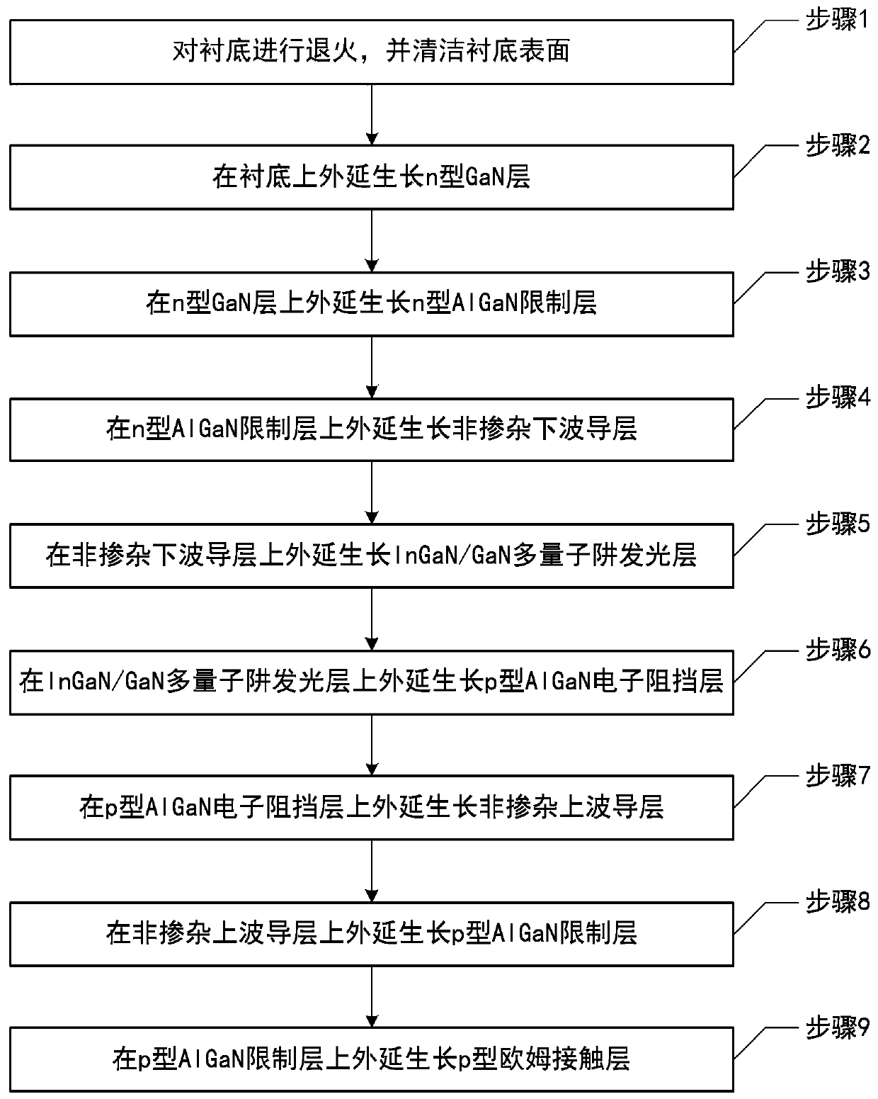
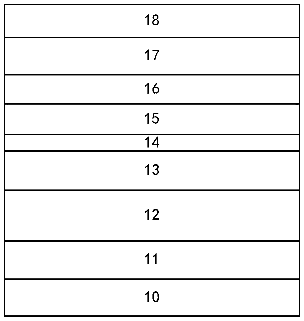
[0032] figure 1 A flow chart of a method for manufacturing a GaN-based multi-quantum well laser epitaxial wafer with low V-type defect density provided by an embodiment of the present disclosure is schematically shown. figure 2 A schematic diagram of the structure of a GaN-based multi-quantum well laser epitaxial wafer provided by an embodiment of the present disclosure with a low V-shaped defect density is schematically shown. combine figure 2 ,right figure 1 Described preparation method is described in detail, and this preparation method comprises:

[0033] Step 1: annealing the substrate 10 and cleaning the surface of the substrate 10 .

[0034] In step 1, the substrate 10 is annealed in a hydrogen atmosphere...


PUM

PropertyMeasurementUnit
thicknessaaaaaaaaaa
thicknessaaaaaaaaaa
emission peakaaaaaaaaaa

Abstract

The invention disclose a GaN-based multi-quantum-well laser epitaxial wafer with low V-type defect density and a preparation method thereof; the preparation method comprises the steps that annealingand surface cleaning are carried out on a substrate (10), and an n-type GaN layer (11), an n-type AlGaN limiting layer (12), an unintentionally-doped lower waveguide layer (13), an InGaN / GaN multi-quantum-well light-emitting layer (14), a p-type AlGaN electron blocking layer (15), an unintentionally-doped upper waveguide layer (16), a p-type AlGaN limiting layer (17) and a p-type ohmic contact layer (18) are grown on the substrate (10) in an epitaxial mode in sequence, wherein the InGaN / GaN multi-quantum-well light-emitting layer (14) comprises an InGaN well layer and a GaN barrier layer; andin growing the GaN barrier layer a TMIn source is pumped so as to inhibit the formation of V-type defects in the GaN barrier layer and eliminate the common V-type defects in the InGaN / GaN multi-quantum wells, so that the reverse electric leakage of the device is reduced, the absorption loss of the device is lowered, and the thermal stability of the quantum well is improved.

Description

technical field [0001] The disclosure relates to the technical field of semiconductor devices, in particular to a GaN-based multi-quantum well laser epitaxial wafer with low V-type defect density and a preparation method thereof. Background technique [0002] The spectrum of GaN-based materials covers the near-infrared to deep ultraviolet bands, and has important application value in the field of optoelectronics, especially GaN-based semiconductor lasers with InGaN low-dimensional structures as active regions, which can realize blue and green laser emission. Among them, the main difficulties faced by green lasers are: (1) The In composition of the InGaN well layer is relatively high, generally 20-30%. The growth of InGaN quantum well materials with high In composition is difficult, the defect density is high, and the luminous efficiency is low; (2) InGaN with high In composition has strong phase segregation, and the composition fluctuates seriously, so that when the high-tem...

Claims


Application Information

Patent Timeline
Patent Type & Authority Patents(China)
IPC IPC(8): H01S5/343
Inventor 杨静赵德刚朱建军陈平刘宗顺梁锋
Owner INST OF SEMICONDUCTORS - CHINESE ACAD OF SCI
Learn More