

Method for preparing DFN package device with high thermal conductivity
A packaging device, high thermal conductivity technology, applied in semiconductor/solid-state device manufacturing, semiconductor device, semiconductor/solid-state device components and other directions, can solve the problems of uneven curing, poor fluidity of epoxy resin composition, and reduced thermal performance, etc. Achieve the effect of improving the heat dissipation effect of the package, improving the heat dissipation effect, and improving the quality of the package
- Summary
- Abstract
- Description
- Claims
- Application Information
AI Technical Summary
Problems solved by technology
Method used
Image

Examples
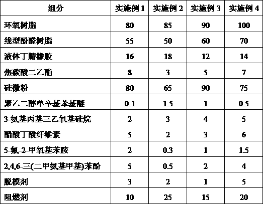
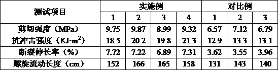
Embodiment 1~4
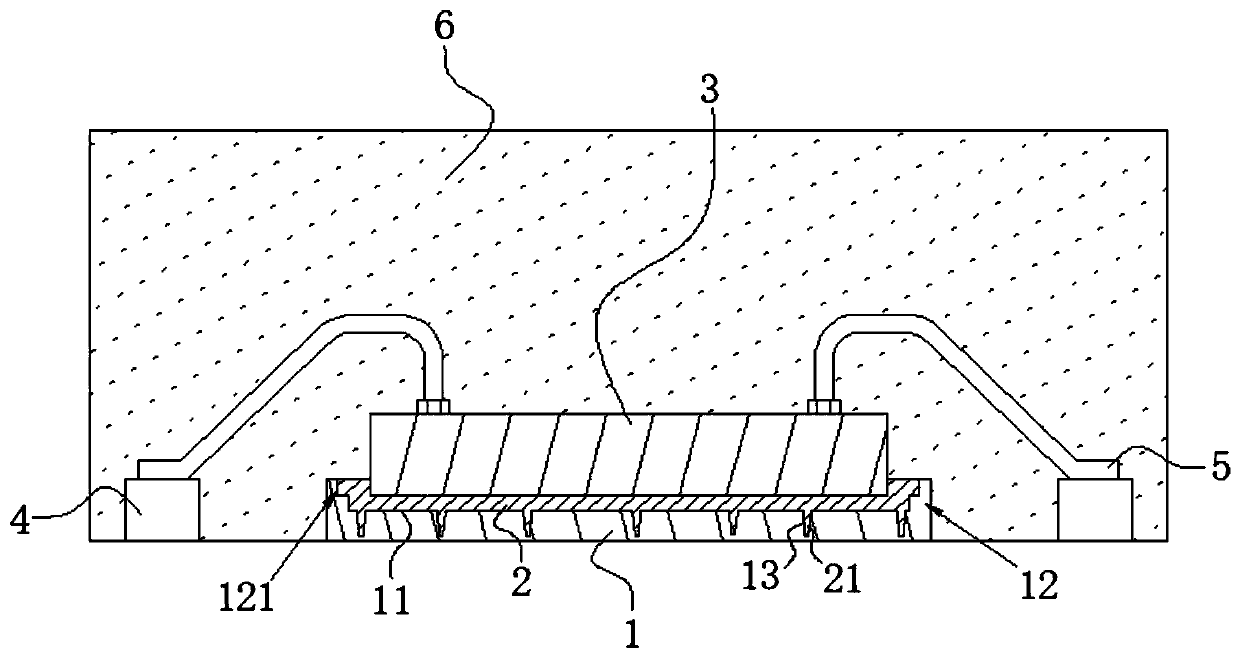
[0027] Embodiments 1 to 4: A preparation method of a high thermal conductivity DFN packaged device, the high thermal conductivity DFN packaged device includes a heat dissipation pad 1, a chip 3 and a conductive pad 4 located in an epoxy insulator 6, and the chip 3 is located in On the heat dissipation pad 1, several conductive pads 4 are arranged around the heat dissipation pad 1, and the conductive pads 4 and the chip 3 are connected by a lead 5;
[0028] The central area of the heat dissipation pad 1 is provided with a sunken groove 11 for embedding the chip 3, thereby forming a cofferdam portion 12 at the edge area of the heat dissipation pad 1, and the bottom of the sunken groove 11 and the cofferdam portion 12 are in contact with the chip. A silver paste layer 2 is provided between the lower surface and the side wall of the 3, and a number of heat exchange blind holes 13 extending into the heat dissipation pad 1 are opened at the bottom of the sinker 11, and in the hea...
Embodiment 1
[0040] The release agent in embodiment 1 is stearic acid, and flame retardant is borate; The release agent in embodiment 2 is stearate, and flame retardant is borate; The release agent in embodiment 3 The agent is oxidized polyethylene wax, and the flame retardant is molybdate; the release agent in Example 4 is a mixture of stearic acid and oxidized polyethylene wax, and the flame retardant is molybdate.
PUM
 Abstract
Description
Claims
Application Information