Vertical GaN Schottky diode device and preparation method thereof
A Gallium Nitride Schottky, vertical technology, applied in the direction of diodes, semiconductor/solid-state device manufacturing, semiconductor devices, etc., can solve the problems of large reverse leakage current, low reverse breakdown voltage, etc., to increase the reverse The effects of improving withstand voltage characteristics, high breakdown voltage, and improving breakdown capability
- Summary
- Abstract
- Description
- Claims
- Application Information
AI Technical Summary
Problems solved by technology
Method used
Image
Examples
Embodiment 1
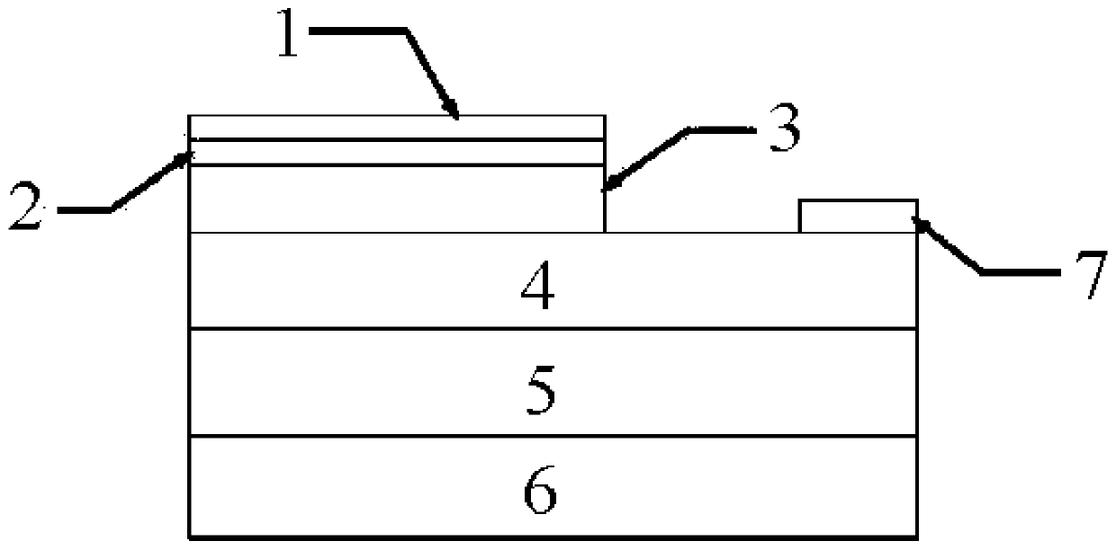
[0055] A preparation method of a gallium nitride Schottky diode device with a quasi-vertical heterostructure:
[0056] Step 1: Deposit a growth buffer layer on the surface of the substrate 6 as the buffer layer 5, and use metal-organic chemical vapor deposition on the buffer layer 5 to form N-type heavily doped layer 4 and N-type lightly doped layer in sequence 3;
[0057] Step 2: Depositing an AlGaN layer 2 on the N-type lightly doped layer 3;
[0058] Step 3: continue to deposit metallic nickel as the anode metal layer 1 by electron beam evaporation technology, and form a Schottky contact with the aluminum gallium nitride layer 2;
[0059] Step 4: Deposit the cathode metal layer 7 on the surface of the N-type heavily doped layer 4 using electron beam evaporation technology, and form an ohmic contact between the two to obtain a gallium nitride Schottky diode device with a quasi-vertical heterostructure, such as figure 1 shown.
Embodiment 2
[0061] A preparation method of a gallium nitride schottky diode device with a quasi-vertical heterostructure with a p-type gallium nitride guard ring:
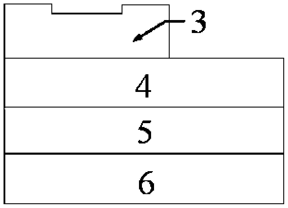
[0062] Step 1: Deposit a growth buffer layer on the surface of the substrate 6 as the buffer layer 5, and use metal-organic chemical vapor deposition on the buffer layer 5 to form N-type heavily doped layer 4 and N-type lightly doped layer in sequence 3, such as figure 2 shown;
[0063] Step 2: Depositing an AlGaN layer 2 on the N-type lightly doped layer 3;
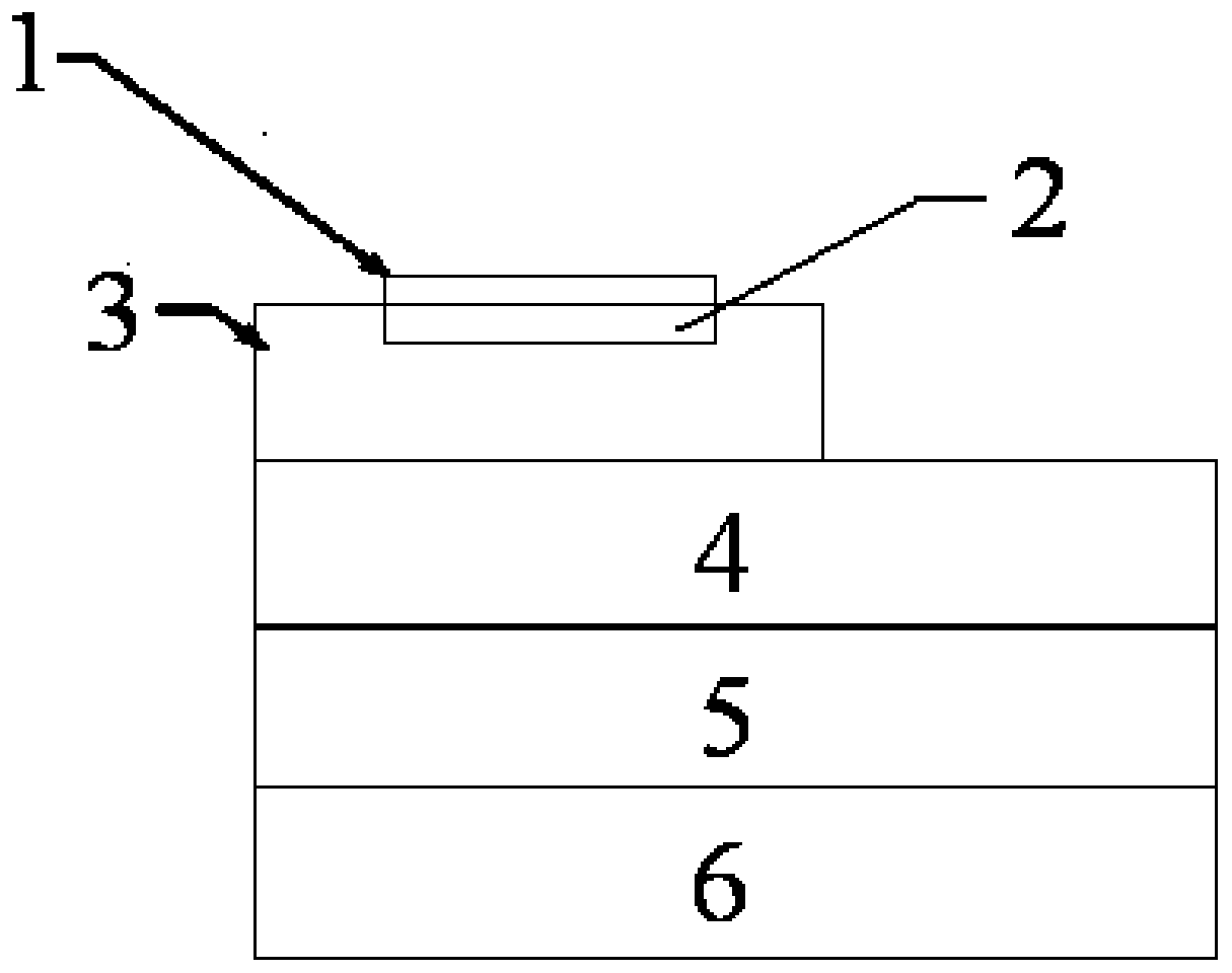
[0064] Step 3: Use electron beam evaporation technology to continue to deposit metallic nickel as the anode metal layer 1, and form a Schottky contact with the aluminum gallium nitride layer 2, such as image 3 shown;
[0065] Step 4: Remove the glue and re-prepare the mask, and prepare a P-type gallium nitride guard ring 8 in the N-type lightly doped layer 3 by using ion implantation technology (the aluminum gallium nitride layer 2 is surrounded by the P-type galliu...
Embodiment 3
[0068] A method for preparing a GaN Schottky diode device with an all-vertical heterostructure:
[0069] Step 1: Deposit a conductive buffer layer on the surface of the substrate 6 (using a conductive substrate) as the buffer layer 5, and use metal-organic chemical vapor deposition on the buffer layer 5 to sequentially form N-type heavily doped layers 4, N-type lightly doped layer 3;
[0070] Step 2: using a photoresist to prepare a mask, etching part of the N-type lightly doped layer 3, etching a groove in the N-type lightly doped layer 3, and depositing an AlGaN layer 2;
[0071] Step 3: On the basis of the original mask, continue to deposit metallic nickel as the anode metal layer 1 by electron beam evaporation technology, and form a Schottky contact with the AlGaN layer 2;
[0072] Step 4: Deposit the cathode metal layer 7 on the surface of the substrate 6 by using electron beam evaporation technology, and form an ohmic contact between the two to obtain a gallium nitride ...
PUM
 Abstract
Description
Claims
Application Information
 - R&D Engineer
- R&D Manager
- IP Professional
- Industry Leading Data Capabilities
- Powerful AI technology
- Patent DNA Extraction
Browse by: Latest US Patents, China's latest patents, Technical Efficacy Thesaurus, Application Domain, Technology Topic, Popular Technical Reports.
© 2024 PatSnap. All rights reserved.Legal|Privacy policy|Modern Slavery Act Transparency Statement|Sitemap|About US| Contact US: help@patsnap.com


