

Diamond coating tool and manufacturing method thereof
A diamond coating and diamond layer technology, applied in metal material coating process, coating, superimposed layer plating and other directions, can solve a large number of diamond fine powder suspension, acid-base waste liquid environmental pollution, uncontrollable number of crystal seeds and other problems, to achieve the effect of improving cutting performance and service life, good cutting performance, and easy industrial production.
- Summary
- Abstract
- Description
- Claims
- Application Information
AI Technical Summary
Problems solved by technology
Method used
Image

Examples
Embodiment 1
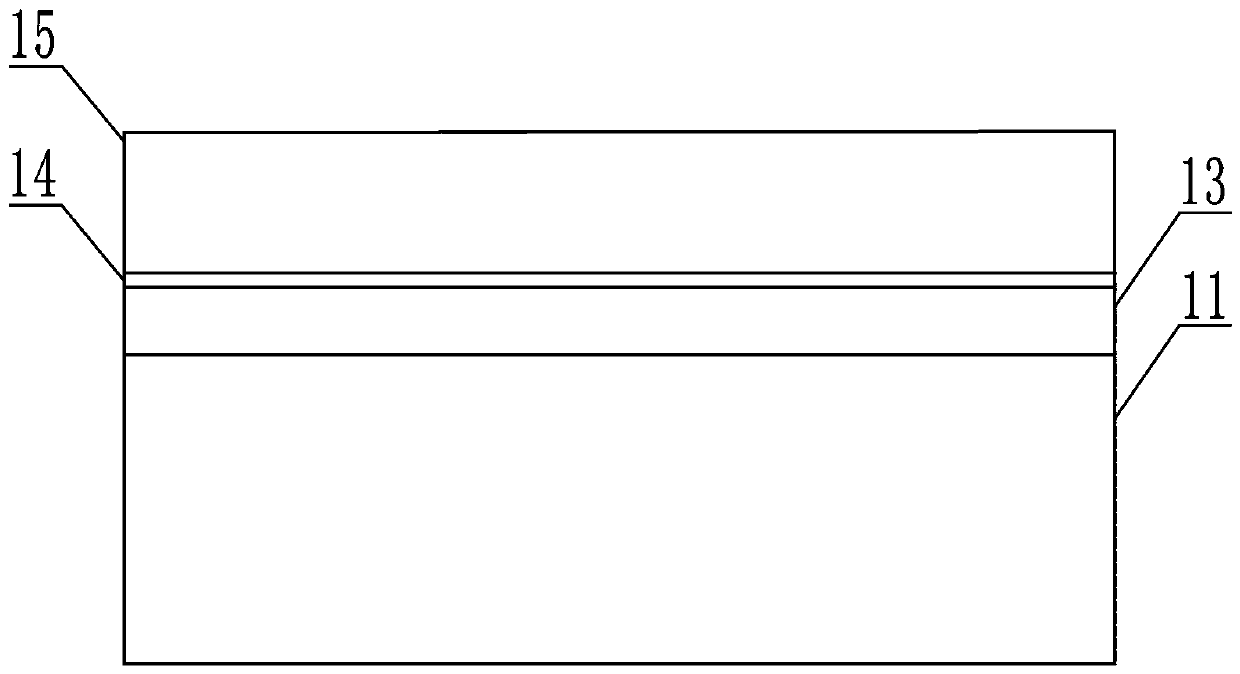
[0029] see figure 1, Embodiment 1 of the present invention provides a diamond-coated tool, which consists of a four-layer structure, specifically including a cemented carbide substrate 11, a TiAlCN layer 13 formed on the upper surface of the cemented carbide substrate 11, and a TiAlCN layer deposited on the TiAlCN layer. The diamond-like layer 14 on the upper surface and the diamond coating 15 formed on the surface of the diamond-like layer 14, wherein, in this embodiment, the cemented carbide substrate 11 is a tungsten-cobalt alloy single-edged blade. The thickness of the TiAlCN layer 13 is 400nm, and the thickness of the diamond-like carbon layer 14 is 25nm. Among them, the TiAlCN layer 13 mainly shields the Co element in the cemented carbide substrate 11 and forms a compound with the Co element to prevent the Co element from diffusing to the upper surface of the cemented carbide substrate 11, so as not to eventually affect the subsequent chemical vapor deposition method. T...
Embodiment 2
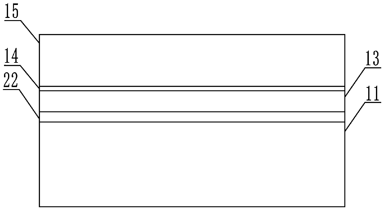
[0039] see figure 2 , the present embodiment provides a diamond-coated cutter, the diamond-coated cutter has a five-layer structure, and its main difference from the diamond-coated cutter provided in Embodiment 1 is that the diamond-coated cutter provided in this embodiment also includes a set In the CrAl layer 22 between the hard alloy substrate 11 and the TiAlCN layer 13, the thickness of the CrAl layer 22 is 200nm, and the CrAl layer 22 is mainly used as a transition layer to increase the thickness of the hard alloy substrate 11 and the TiAlCN layer. The binding force of the TiAlCN layer 13; in the present embodiment, the superhard alloy substrate 11 is a common alloy two-edged cutter, the thickness of the TiAlCN layer 13 is 300nm, and the thickness of the diamond-like layer 14 is 20nm, so The thickness of the diamond layer 15 is 8 μm.
[0040] This embodiment also provides a method for preparing the above-mentioned diamond-coated cutting tool, including:
[0041] Cleani...
Embodiment 3
[0049] This embodiment provides a diamond-coated tool and a preparation method thereof, which are basically the same in structure and preparation method of the diamond-coated tool provided in Example 2, except that the thicknesses of each coating and the diamond layer are different; Specifically, in this embodiment, the thickness of the CrAl layer is 250nm, and the deposition time is 15min; the thickness of the TiAlCN layer is 200nm, and the deposition time is 10min; the thickness of the diamond-like layer is 10nm, and the deposition time is 10min; The thickness of the layer is 10 μm, and the reaction time is 20 h.
PUM
| Property | Measurement | Unit |
|---|---|---|
| Thickness | aaaaa | aaaaa |
| Thickness | aaaaa | aaaaa |
| Thickness | aaaaa | aaaaa |
Abstract
Description
Claims
Application Information