Preparation method and application of polymer semiconductor film
A thin film preparation and semiconductor technology, which is applied in the field of polymer semiconductor film preparation, can solve the problems of difficult large-area preparation, time-consuming and laborious, etc., and achieve the effect of simple preparation method, simple and fast experimental process, and avoiding the formation of coffee rings
- Summary
- Abstract
- Description
- Claims
- Application Information
AI Technical Summary
Problems solved by technology
Method used
Image

Examples
Embodiment 1
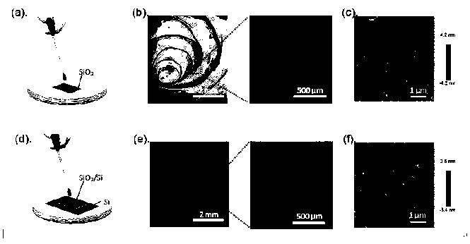
[0042] Embodiment 1, prepare the PCDTPT film semiconductor preparation based on silicon dioxide substrate
[0043] (1) Preparation of PCDTPT polymer semiconductor solution
[0044] Using chloroform as a solvent and PCDTPT polymer powder as a solute, a PCDTPT semiconductor solution with a concentration of 0.25 mg / ml was prepared. Note that during the solution preparation process, it is necessary to strictly ensure that any tools in contact with drugs and solvents have a high degree of cleanliness, and at the same time, no plastic tools or containers can be used to contact solvents or solutions. The specific operation is as follows: Take a brown bottle with a volume of 20ml and clean it for later use. Use an electronic balance to weigh 2.5mg of PCDTPT polymer powder and place it in the bottle. Use a glass dropper and a graduated cylinder to take 10ml of chloroform solution and mix it with the solute. Put the cleaned rotor into the solution, place it on the turntable and stir fo...
Embodiment 2
[0058] Embodiment 2, preparation of PCDTPT polymer semiconductor thin film preparation based on Si substrate
[0059] (1) Preparation of PCDTPT polymer semiconductor solution
[0060] Using chloroform as a solvent and PCDTPT polymer powder as a solute, a PCDTPT semiconductor solution with a concentration of 0.25 mg / ml was prepared. Same as embodiment 1 step (1)
[0061] (2) Si substrate preparation and target substrate hydroxylation treatment
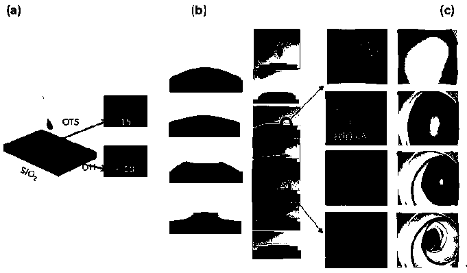
[0062] First, the Si substrate was cut into squares of 2 cm x 2 cm and 0.5 cm x 0.5 cm with a glass knife and cleaned. The cleaning process was the same as step (1) in Example 1. The 0.5cm×0.5cm SiO 2 The substrate is used as the upper target substrate of the laminated structure, and the Si substrate is placed in the piranha washing solution (a mixed solution of concentrated sulfuric acid with a mass concentration of 98% and hydrogen peroxide with a mass concentration of 30% at a volume ratio of 7:3) , form hydroxylation on the surf...
Embodiment 3
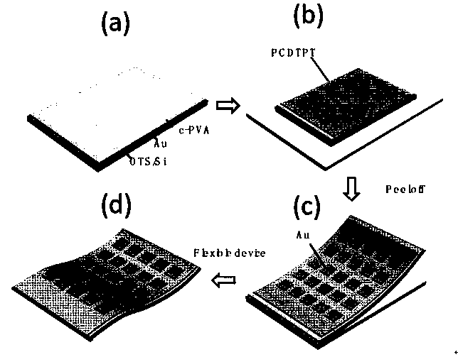
[0072] Example 3, preparation of PCDTPT polymer semiconductor thin film based on flexible PVA substrate and preparation of ultra-thin flexible field-effect transistor
[0073] (1) Cross-linked PVA solution configuration
[0074] Dissolve PVA powder in secondary deionized water at a concentration of 6wt%, heat and stir to dissolve. In order to enhance the solvent resistance of the substrate, the cross-linking agent glutaraldehyde is added after dissolving evenly for cross-linking (mixing volume ratio 200:3), and the cross-linked PVA is formed after continuing to stir evenly.
[0075] (2) Preparation of PCDTPT polymer semiconductor solution
[0076] Using chloroform as a solvent and PCDTPT polymer powder as a solute, a PCDTPT semiconductor solution with a concentration of 0.25 mg / ml was prepared. Same as embodiment 1 step (1)
[0077] (3) PVA substrate preparation and target substrate hydroxylation treatment
[0078] 3-1) Firstly, the Si substrate was cut into squares of 2 c...
PUM
| Property | Measurement | Unit |
|---|---|---|
| Thickness | aaaaa | aaaaa |
Abstract
Description
Claims
Application Information
 - R&D
- Intellectual Property
- Life Sciences
- Materials
- Tech Scout
- Unparalleled Data Quality
- Higher Quality Content
- 60% Fewer Hallucinations
Browse by: Latest US Patents, China's latest patents, Technical Efficacy Thesaurus, Application Domain, Technology Topic, Popular Technical Reports.
© 2025 PatSnap. All rights reserved.Legal|Privacy policy|Modern Slavery Act Transparency Statement|Sitemap|About US| Contact US: help@patsnap.com