Zinc oxide-porous silicon composite material and preparation method and application thereof
A technology of composite materials and porous silicon, applied in nanotechnology for materials and surface science, hybrid capacitor electrodes, nanotechnology, etc., can solve the problems of active chemical properties and poor capacitance characteristics of porous silicon surface, and facilitate industrialization The effect of application, improvement of capacitance characteristics, and simple preparation process
- Summary
- Abstract
- Description
- Claims
- Application Information
AI Technical Summary
Problems solved by technology
Method used
Image


Examples
preparation example Construction
[0034] A preparation method of zinc oxide-porous silicon composite material, comprising the following steps:
[0035] material selection:
[0036] The resistance of the selected silicon chip is 1-10Ωcm 2 And p-type single crystal silicon with a crystal orientation of [100], single-sided polishing.
[0037] Preparation of porous silicon:
[0038] Pretreatment of silicon wafers: sputtering a layer of metal aluminum film on the surface of single crystal silicon to ensure good electrical conductivity between the back of the silicon substrate and the metal anode. Cut the pretreated silicon wafers into 14mm×14mm squares, use acetone, alcohol, and deionized water to ultrasonically clean the silicon surface to remove impurities, and then use dilute HF acid to soak and rinse to remove the surface oxide layer. The electrolyte is a mixed solution of 40% hydrofluoric acid HF, absolute ethanol and N,N-dimethylformamide DMF; preferably, the hydrofluoric acid HF, absolute alcohol and N,N-...
Embodiment 1
[0050] This embodiment is a preferred embodiment of the method for preparing the zinc oxide-porous silicon composite material of the present invention, including the following steps:
[0051] Select material: silicon chip resistance is 1-10Ωcm 2 And p-type single crystal silicon (single-side polished) with a crystal orientation of [100].
[0052] Preparation of porous silicon: pretreat the silicon wafer, and sputter a layer of metal aluminum film with a thickness of about 800nm on the surface of the single crystal silicon to ensure good conductivity between the back of the silicon substrate and the metal anode. Subsequently, the pretreated silicon wafers were cut into squares of 14mm×14mm. Then use acetone, alcohol, and deionized water to ultrasonically clean to remove impurities on the silicon surface, and then use dilute HF acid to soak and rinse to remove the surface oxide layer. Electrolyte selects the mixed solution of 40% hydrofluoric acid HF, dehydrated alcohol and ...
Embodiment 2
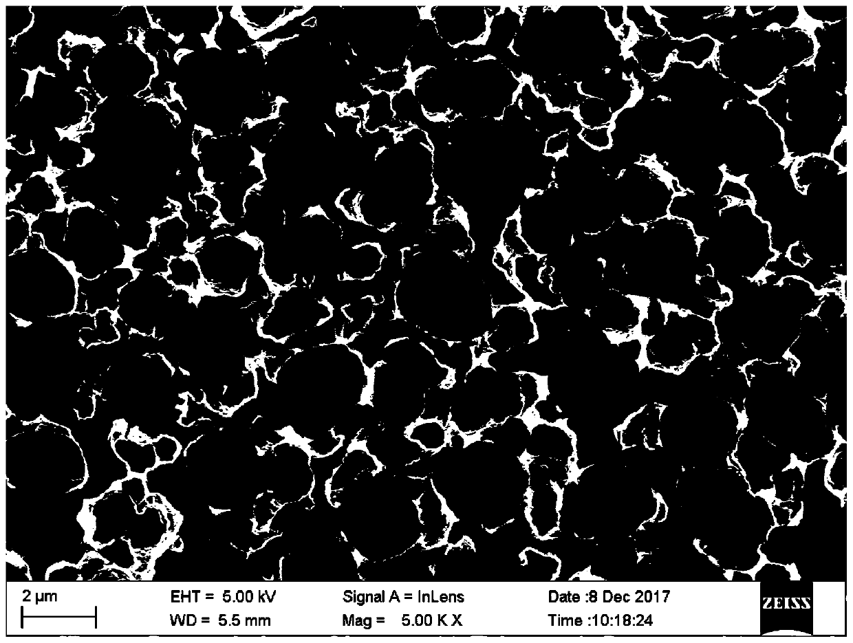
[0065] This Example 2 is a comparison of Example 1. The difference between this Example 2 and Example 1 is that the preparation of the zinc oxide-porous silicon composite material in this Example 2 is prepared by using the traditional hydrothermal growth method. During preparation, a certain amount of sol liquid is firstly injected into the hydrothermal synthesis reactor, and the prepared porous silicon sample is sealed with a heat-resistant and waterproof sealant at the part that does not need to be compounded, and then the porous silicon sample is put into the reactor. Set the temperature of the transverse oven at 120°C, take out the sample after 8 hours of heat preservation, wash and dry to obtain the zinc oxide-porous silicon composite material.
[0066] Result analysis:
[0067] Figure 9 (a) and (b) are the SEM characterization results of the zinc oxide-porous silicon composite prepared by the hydrothermal growth method. It can be easily found that the porous silicon surf...
PUM
 Abstract
Description
Claims
Application Information
 - R&D
- Intellectual Property
- Life Sciences
- Materials
- Tech Scout
- Unparalleled Data Quality
- Higher Quality Content
- 60% Fewer Hallucinations
Browse by: Latest US Patents, China's latest patents, Technical Efficacy Thesaurus, Application Domain, Technology Topic, Popular Technical Reports.
© 2025 PatSnap. All rights reserved.Legal|Privacy policy|Modern Slavery Act Transparency Statement|Sitemap|About US| Contact US: help@patsnap.com