
Organic photoelectric detector and manufacturing method thereof

A photodetector and organic technology, applied in photovoltaic power generation, electric solid-state devices, semiconductor/solid-state device manufacturing, etc., can solve the problems of material failure, easy carbonization of organic materials, high cost, etc., to reduce production costs, low cost, avoid The effect of negative electrode recombination

Inactive Publication Date: 2019-10-18
SHANGHAI UNIV
View PDF13 Cites 2 Cited by
  • Summary
  • Abstract
  • Description
  • Claims
  • Application Information

AI Technical Summary

Problems solved by technology

[0004] In the prior art, when preparing organic photodetectors, it needs to be prepared through complex processes such as high-vacuum evaporation or high-temperature annealing and crystallization. The organic materials are easily carbonized at high temperatures, resulting in material failure and high cost. High-quality and long-life new-generation photodetection and imaging technology basic devices are developing. A new generation of photodetection devices with simple preparation process, low cost, high mechanical properties, and suitable for the preparation of flexible wearable devices has become an urgent technical problem to be solved.

Method used


Image

  • Organic photoelectric detector and manufacturing method thereof
  • Organic photoelectric detector and manufacturing method thereof

Examples


Embodiment 1

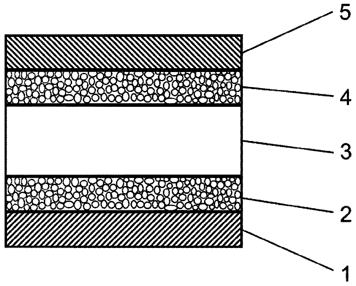
[0038] In this example, see figure 1 , an organic photodetector, sequentially composed of a substrate, a negative electrode ITO conductive film layer 1, a first functional layer 2, an organic active working layer 3, a second functional layer 4, and a positive electrode layer 5 to form a multilayer device structure. The active working layer 3 is made of a bulk heterojunction mixed material, which absorbs the detection light and forms photogenerated carriers;

[0039] The first functional layer 2 serves as an electron transport layer and as a hole blocking layer;

[0040] The second functional layer 4 acts as a hole transport layer and as an electron blocking layer;

[0041] The first functional layer 2, the organic active working layer 3, and the second functional layer 4 all use a solution method, using a nanoparticle dispersion containing a volatile solvent, and then preparing a nanomaterial film by a spin coating method, and then preparing a thin film of nanomaterials at no...

Embodiment 2

[0055] This embodiment is basically the same as Embodiment 1, especially in that:

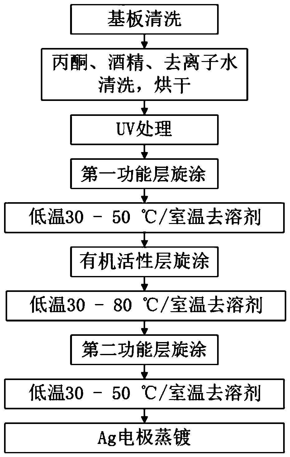
[0056] In this embodiment, a method for preparing an organic photodetector of this embodiment includes the following steps:

[0057] a. Preparation of negative electrode ITO conductive film layer:

[0058] Through the sputtering process, the nano-silver particle material layer is deposited on the ITO glass substrate or the ITO flexible substrate, and then the acetone, alcohol, and deionized water are respectively ultrasonicated for 10 minutes, then dried, and then subjected to UV treatment to strengthen the surface of the substrate. Combined with the nano-silver particle material layer to prepare the negative electrode ITO conductive film layer;

[0059] b. Preparation of the first functional layer:

[0060] By means of spin coating, the nanoparticle dispersion liquid containing volatile solvent is used as the coating material, and the nanometer film layer is coated on the nanosilver particle...

Embodiment 3

[0069] This embodiment is basically the same as the previous embodiment, and the special features are:

[0070] In this embodiment, a method for preparing an organic photodetector of this embodiment includes the following steps:

[0071] a. Preparation of negative electrode ITO conductive film layer:

[0072] Through the sputtering process, the nano-silver particle material layer is deposited on the ITO glass substrate or the ITO flexible substrate, and then the acetone, alcohol, and deionized water are respectively ultrasonicated for 10 minutes, then dried, and then subjected to UV treatment to strengthen the surface of the substrate. Combined with the nano-silver particle material layer to prepare the negative electrode ITO conductive film layer;

[0073] b. Preparation of the first functional layer:

[0074] By the way of spin coating, adopt the nano particle dispersion liquid that contains volatile solvent as coating material, on the nano silver particle material layer o...


PUM


Abstract

The invention discloses an organic photoelectric detector and a manufacturing method thereof. A main functional layer is prepared by solution spin coating. The method has simple process, low cost andhigh mechanical property and is suitable for preparing a flexible wearable device. Functional layer materials are all nanoparticle dispersions, solvent of the dispersions is volatile solvent, the solvent can be removed at low temperature or at room temperature after spin coating, an efficient device functional layer material is formed, the complicated process such as high vacuum evaporation or high temperature annealing crystallization is not needed, cost is low, and the method is more suitable for large-scale manufacturing. The active layer organic material is a bulk heterojunction PN-junction material, and the material can be in effective contact with a variety of functional layer materials and can form function matching with the functional layer material. The method is advantaged in that the method is simple, preparation can be achieved at low temperature or at room temperature, the process requirements are low, cost is low, mechanical performance is good, and the method is suitablefor preparing rigid and flexible substrate devices.

Description

technical field [0001] The invention relates to a photoelectric device and a preparation method thereof, in particular to an organic photoelectric device and a preparation method thereof, which are applied in the technical fields of light detection and imaging. Background technique [0002] Optoelectronics technology covers a wide range of technical fields. It not only involves the generation of optical signals, but also involves the reception and detection of optical signals. It converts the received optical radiation into another type of physical quantity that is easy to operate and measurable , usually converted into electricity to achieve the ultimate goal of target detection. Photoelectric detection and imaging is an important branch of the current application of optoelectronic technology, which can clearly image the target and meet the needs of military and civil applications. Photoelectric imaging devices need to meet the following requirements: higher sensitivity to...

Claims


Application Information

Patent Timeline
Patent Type & Authority Applications(China)
IPC IPC(8): H01L51/42H01L51/44H01L51/48H01L51/00H10K99/00
CPCH10K71/12H10K30/20H10K30/80Y02E10/549
Inventor 张建华李意
Owner SHANGHAI UNIV
Learn More