
tio 2 Thin film preparation method, photodetector device and preparation method thereof

A photodetector and photodetection technology, applied in electrical components, semiconductor devices, circuits, etc., can solve problems such as difficulty in obtaining TiO single crystal thin films, inability to control spectral response, and weak performance of photodetection devices, so as to reduce oxygen defects , reduce the effect of recombination and concentration

Active Publication Date: 2021-04-09
SHENZHEN TECH UNIV
View PDF6 Cites 0 Cited by
  • Summary
  • Abstract
  • Description
  • Claims
  • Application Information

AI Technical Summary

Problems solved by technology

[0005] However, TiO prepared using existing preparation methods 2 Most of the thin film materials are amorphous or polycrystalline materials, and it is difficult to obtain TiO 2 Single crystal thin film, so the performance of the prepared photodetector device is weak, and it cannot have the ability to control the spectral response

Method used


Image

  • tio  <sub>2</sub> Thin film preparation method, photodetector device and preparation method thereof
  • tio  <sub>2</sub> Thin film preparation method, photodetector device and preparation method thereof
  • tio  <sub>2</sub> Thin film preparation method, photodetector device and preparation method thereof

Examples


preparation example Construction

[0036] Embodiments of the present invention propose a crystallized TiO 2 The preparation method of thin film, comprises the following steps:

[0037] S1, using nitrogen as the load gas, alternately feeding titanium source and water vapor, and obtaining atomic-level TiO generated by the reaction on the oxide layer of the substrate 2 , the reaction temperature is 220-300°C, and the reaction pressure is 10-20 Pa;

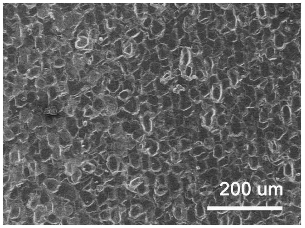
[0038] S2, TiO obtained from S1 2 The substrate is calcined in an oxygen-containing atmosphere at a temperature of 400-800°C, that is, crystallized fish-scale TiO is obtained on the substrate. 2 film, such as image 3 shown;

[0039] Wherein, the titanium source is titanium isooxypropoxide (Ti{OCH(CH 3 ) 2} 4 ), the temperature of the titanium source is 70-80°C;

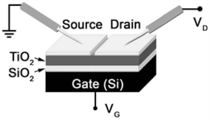
[0040] The substrate is P-type Si with a silicon oxide layer on one side and Si on the other side.

[0041] In one embodiment, argon is used as a carrier gas, and titanium source and water vapor are ...

experiment example

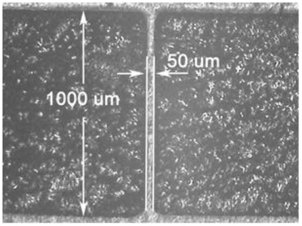
[0074] Experimental example: Substrate pretreatment: first treat the substrate SiO 2 / P-Si preparation and cleaning. First, use electronic cleaning agent diluent, ethanol, and deionized water for preliminary washing; then use ammonia water, hydrogen peroxide, and deionized water to form a mixed solution at a ratio of 1:1:5, and put the silicon wafer into the mixed solution for ultrasonic cleaning After 15 minutes, use deionized water for multiple ultrasonic cleaning to remove the washing residue until the washing liquid after washing is detected as neutral by pH test paper; then use concentrated hydrochloric acid, hydrogen peroxide, and deionized water according to the ratio of 1:1:5 Ratio to form a mixed solution, put the silicon chip into the mixed solution for ultrasonic cleaning for 15 minutes, and then use deionized water to ultrasonically clean it several times to remove the washing residue until the washing solution after washing is detected as neutral by pH test paper;...


PUM


Abstract

The invention discloses a TiO 2 A thin film preparation method, a photoelectric detection device and a preparation method thereof relate to the technical field of photoelectric detection. The present invention utilizes TiO produced by calcining ALD (atomic layer layer-by-layer deposition) in an oxygen-containing environment 2 thin film, on the one hand makes the TiO 2 The film changes from amorphous to local single crystal, forming a fish-scale appearance; on the other hand, reducing oxygen defects, reducing the concentration of electrons in the material, reducing the recombination of photogenerated carriers, which is conducive to the formation of photocurrent and also reduces dark current. The size of the photodetector device made of this material enables the device to improve the performance of photodetection; the device has the ability to regulate the spectral response of the gate voltage.

Description

technical field [0001] The invention relates to the technical field of photoelectric detection, in particular to a TiO 2 A thin film preparation method, a photodetector device and a preparation method thereof. Background technique [0002] In modern photoelectric detection technology, photodetectors can find relevant applications in many fields, including environmental security, information technology, medical treatment, astronomical observation and military applications, and satellite communications. After the laser detection technology and infrared detection technology, the ultraviolet band has attracted more and more attention, and it has developed another extremely important photoelectric detection technology. Foreign countries have begun military research on ultraviolet technology, and have made some progress, such as ultraviolet guidance, ultraviolet early warning, ultraviolet interference and ultraviolet communication. Metal nitrides and oxides are often used as wid...

Claims


Application Information

Patent Timeline
Patent Type & Authority Patents(China)
IPC IPC(8): H01L31/032H01L31/113H01L31/18C23C16/02C23C16/40C23C16/455C23C16/56
CPCC23C16/0227C23C16/405C23C16/45525C23C16/56H01L31/0324H01L31/1136H01L31/18Y02P70/50
Inventor 季涛胡俊青胡鑫余利张昊艾福金
Owner SHENZHEN TECH UNIV
Learn More