Novel nanostructure thin film solar cell and its preparation method

A technology for solar cells and nano-silicon thin films, applied in circuits, electrical components, photovoltaic power generation, etc., can solve the problem of unfavorable photoelectric performance, affecting the illumination range of incident light, and low photoelectric conversion efficiency of nano-silicon-amorphous silicon heterojunction solar cells. And other issues

Active Publication Date: 2021-08-20
何金明
View PDF5 Cites 0 Cited by
  • Summary
  • Abstract
  • Description
  • Claims
  • Application Information

AI Technical Summary

Problems solved by technology

[0003] For traditional nano-silicon-amorphous silicon heterojunction solar cells, the thickness of the active layer (nano-silicon film) is relatively small, which affects its light absorption performance, resulting in nano-silicon-amorphous silicon heterojunction solar cells Photoelectric conversion efficiency is relatively low (2-3%)
In addition, traditional nano-silicon-amorphous silicon heterojunction solar cells use top electrodes such as aluminum, gold or gold / nickel alloys. Although a grid structure is used in the electrode preparation process, it still inevitably affects the incident light. The light range is not conducive to its photoelectric performance

Method used


Image

  • Novel nanostructure thin film solar cell and its preparation method
  • Novel nanostructure thin film solar cell and its preparation method
  • Novel nanostructure thin film solar cell and its preparation method

Examples


Embodiment Construction

[0027] The invention is further illustrated in conjunction with the accompanying drawings and specific embodiments.

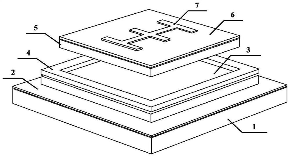
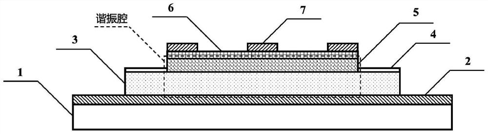
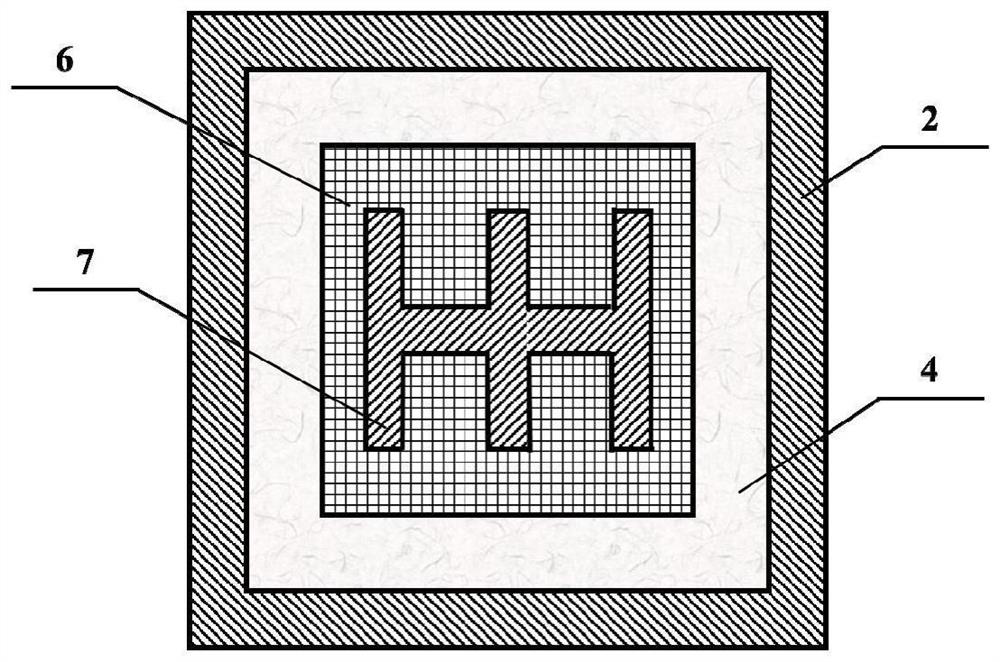
[0028] This example provides a flat thin film solar cell of a graphene junction structure, such as a graphene junction structure, such as Figure 1-3 As shown, a quartz or glass substrate 1, an Al electrode 2, a phosphorus doped amorphous silicon film 3, a silicon carbide film interface layer 4, a boron doped nano film 5, a graphene layer 6, and a graphene layer 6, and a graphene layer 6. AU electrode 7; phosphorus doped amorphous silicon film between the graphene layer and the Al electrode, a boron doped nano film constitutes a nano-resonant cavity. The nano-resonant cavity calculates the thickness of the p-type nanocaricon / N-type amorphous silicon heterojunction by measuring the refractive index and reflectance of graphene, phosphorus doped amorphous silicon, boron doped nanothermium and aluminum. The visible light satisfies the resonance condition in the nanowa...


PUM

PropertyMeasurementUnit
thicknessaaaaaaaaaa
thicknessaaaaaaaaaa
thicknessaaaaaaaaaa

Abstract

The invention discloses a novel nanostructure thin-film solar cell, comprising a quartz or glass substrate, an Al electrode, a phosphorus-doped amorphous silicon film, a silicon carbide film interface layer, a boron-doped nano-silicon film, Graphene layer and Au electrodes. The resonant cavity mechanism is used to enhance the light absorption in the p-type nano-silicon / n-type amorphous silicon heterojunction, thereby improving the optoelectronic performance of the device. Compared with the traditional silicon-based thin-film solar cell, the production cost of the graphene / p-type nano-silicon / n-type amorphous silicon heterojunction planar thin-film solar cell provided by the present invention can be saved by 30%. The design and preparation process of the battery is simple, the material consumption is low, and high-temperature sintering treatment is avoided in the production process, which greatly reduces the production energy consumption of silicon-based thin-film solar cells, and can effectively reduce the production cost of traditional silicon-based thin-film solar cells.

Description

Technical field [0001] The present invention relates to a nano-nanostructured thin film solar cell, and more particularly to a planar film solar cell based on a resonant chamber-based mechanism, a planar film solar cell and a preparation method thereof, Optoelectronic technology field. Background technique [0002] With the continuous development of the new generation of solar cells, the nano-silicon structure is considered to be a material capable of better regulating the width of the ban, wherein the use of the nano silicon structure and the heterojunction of the single crystal silicon substrate. Solar batteries have always been a popular research hotspot. However, since the thickness of the silicon active layer is very thin with respect to the single crystal silicon substrate, the absorption of the sunlight is limited, and therefore, most of the light carriers are from the single crystal silicon substrate rather than nanoicon silicon. The active layer and nanoilage have not be...

Claims


Application Information

Patent Timeline
Patent Type & Authority Patents(China)
IPC IPC(8): H01L31/0445H01L31/072H01L31/18
CPCH01L31/072H01L31/18H01L31/0445Y02E10/50Y02P70/50
Inventor 单丹周寿斌唐明军杨瑞洪曹蕴清钱松陈雪圣
Owner 何金明
Why Eureka
Try Eureka