

Indium sulfide-based impurity band semiconductor and preparation method and application thereof
A semiconductor and impurity technology, applied in the field of new semiconductor materials, can solve the problems of limited photoelectric conversion efficiency of solar cells, weak conductivity of indium trisulfide semiconductor, ineffective utilization of photons, etc., to achieve efficient utilization, simple preparation method, and improved The effect of solar energy absorption
- Summary
- Abstract
- Description
- Claims
- Application Information
AI Technical Summary
Problems solved by technology
Method used
Image

Examples
Embodiment
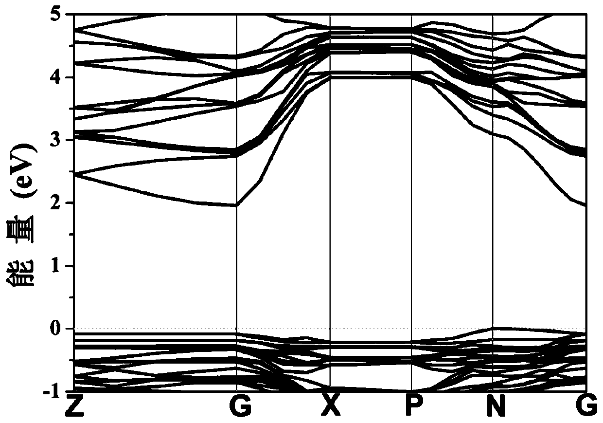
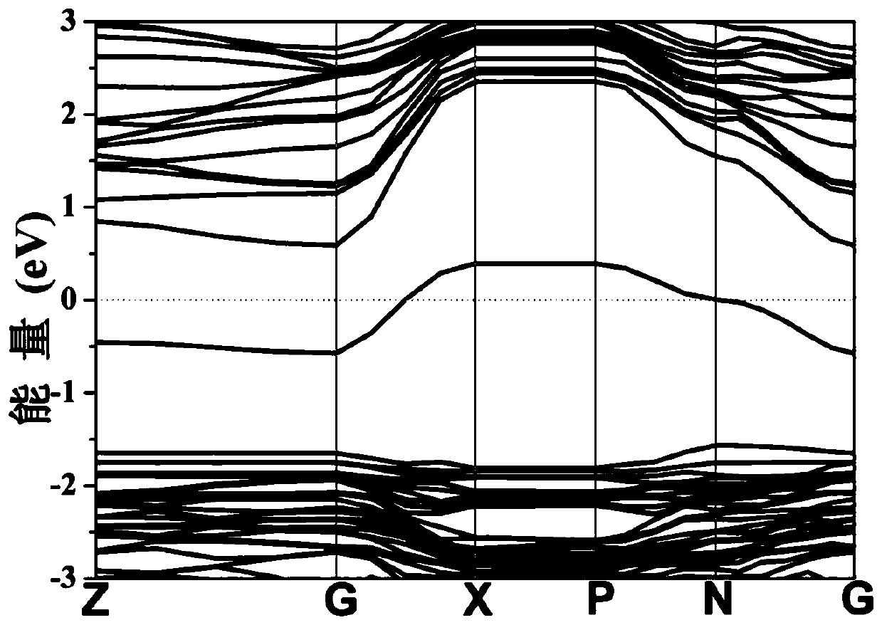
[0029] In the present invention In 2-x Ge x S 3 (x is reasonably set according to the doping ratio) The samples are all sintered by vacuum solid-state reaction. According to the stoichiometric ratio, In particles, S powder, and Ge powder are vacuum-packed in a quartz tube, and the temperature is slowly raised to 850°C and kept for more than 24 hours. Finally, the sample is cooled with the furnace to obtain Ge element-doped In 2 S 3 Semiconductor In 2-x Ge x S 3 .
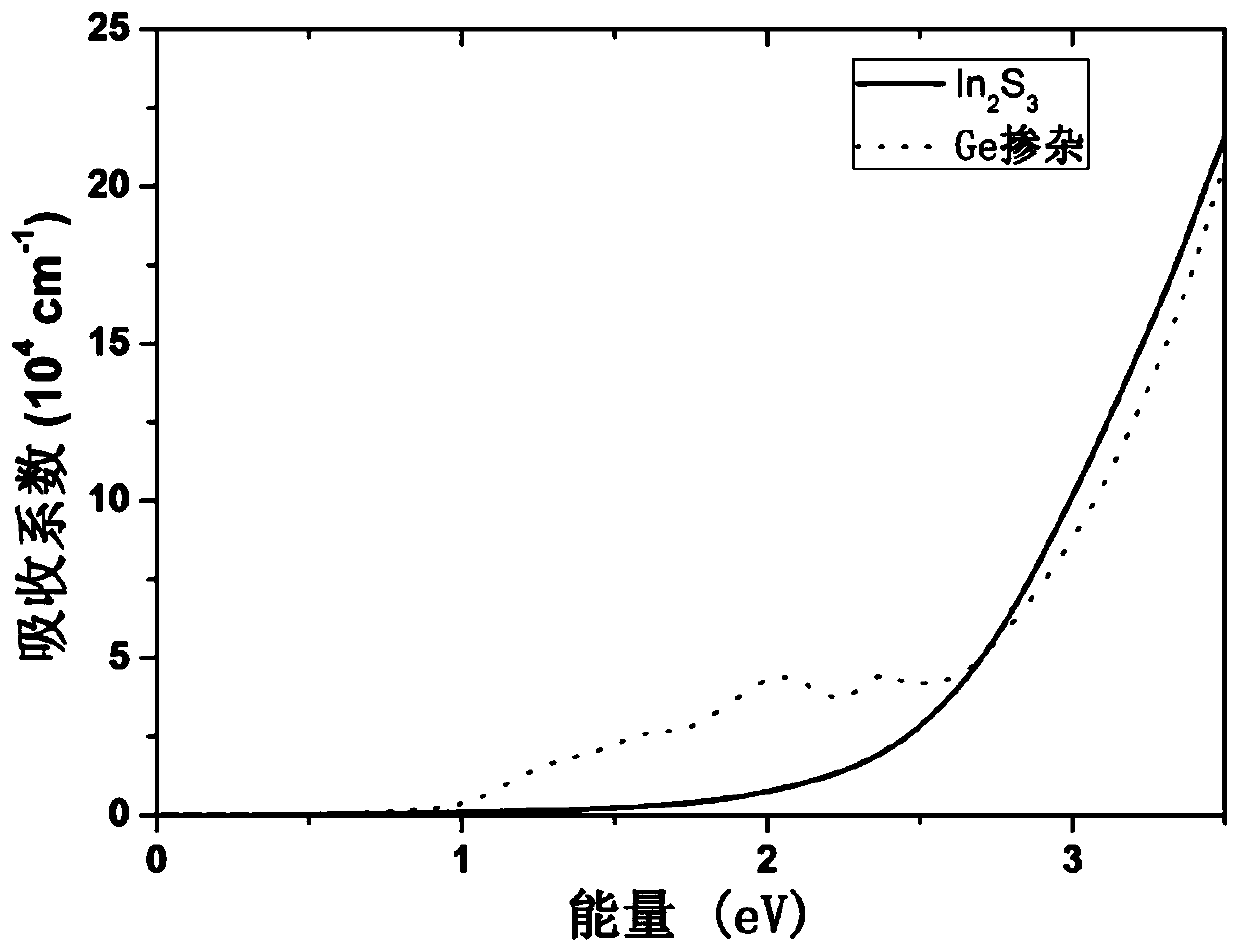
[0030] In the present invention 2 S 3 As the parent body, the energy band structure is adjusted by doping Ge elements at the In site, and the intermediate impurity band is introduced, so that electrons can not only jump directly from the valence band to the conduction band, but also enable electrons to absorb photons whose energy is less than the forbidden band width to jump to impurities. The band reabsorbs a lower-energy photon to transition to the conduction band, thereby broadening the absorption spectr...
PUM
 Abstract
Description
Claims
Application Information