AlGaN-based ultraviolet LED device and preparation method and application thereof

A technology of LED devices and epitaxial layers, applied in semiconductor devices, electrical components, circuits, etc., can solve the problems of large surface roughness, high film content, and no phase separation of components involved, and achieve the carrier-limited threshold effect. , increasing the radiation recombination efficiency and improving the surface morphology of the film

Active Publication Date: 2019-11-15
NINGBO INST OF MATERIALS TECH & ENG CHINESE ACADEMY OF SCI +1
View PDF25 Cites 6 Cited by
  • Summary
  • Abstract
  • Description
  • Claims
  • Application Information

AI Technical Summary

Problems solved by technology

[0004] EP03254642.6 prepared a lateral pn junction LED, which can only regulate the flow direction of carriers in the macroscopic area, and cannot realize the In-rich "quantum dots" similar to InGaN LEDs on the microscopic level.
US15177608 uses nanowire LEDs to improve luminous efficiency, but has the disadvantage of poor electrical properties of low-dimensional nanomaterials and cannot be industrialized on a large scale
CN201180018207.6 fully adopts nitrogen polarity as LED epitaxial film, the main disa

Method used


Image

  • AlGaN-based ultraviolet LED device and preparation method and application thereof
  • AlGaN-based ultraviolet LED device and preparation method and application thereof
  • AlGaN-based ultraviolet LED device and preparation method and application thereof

Examples


preparation example Construction

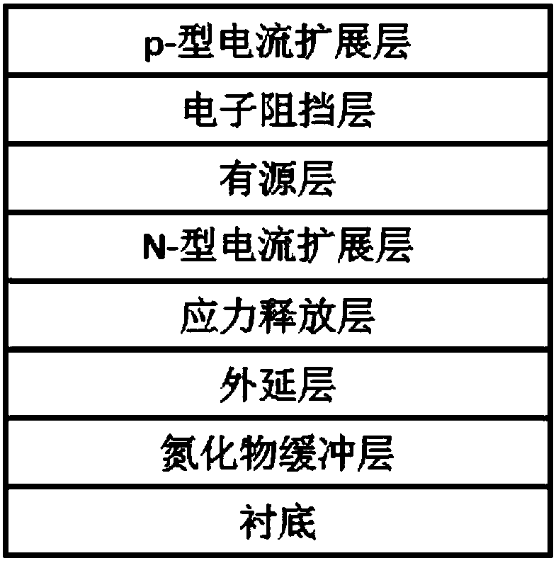
[0026] An aspect of the embodiments of the present invention provides a method for manufacturing an AlGaN-based ultraviolet LED device, which includes:

[0027] growing and forming a nitride buffer layer on the substrate, and pretreating the nitride buffer layer, wherein the pretreatment includes any one of plasma treatment, high temperature thermal annealing treatment and metal organic source precursor pretreatment or a combination of two or more; then sequentially form an epitaxial layer, a stress release layer, an n-type current spreading layer, a multilayer quantum well active layer, an electron blocking layer and a p-type current spreading layer on the nitride buffer layer .

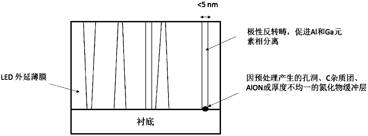
[0028] The mechanism that the present invention carries out pretreatment to nitride buffer layer may be: see figure 2 As shown, plasma treatment, high-temperature annealing, or pretreatment of nitride buffer film with MO precursors cause fluctuations in the film thickness of the buffer layer, resu...

Embodiment 1

[0064] A 10nm thick AlN buffer film was deposited on a sapphire substrate (2 inches in diameter and 430 microns in thickness) based on low-temperature MOCVD, and the deposition temperature of the buffer layer was 800°C. Use plasma treatment for 10min, etching conditions are 10mtorr, RF / ICP: 100 / 300W, Cl / BCl 3 : 10 / 25 sccm. Afterwards, put the substrate back into the MOCVD chamber, grow an AlN epitaxial layer of 50nm at high temperature, the growth temperature is 1200°C, V / III=300, then lower the temperature to 1150°C, keep the pressure at 200torr, and grow a 700nm thick AlN epitaxial layer 0.7 Ga 0.3 N to Al 0.3 Ga 0.7 A stress relief layer with gradually decreasing N-Al components. Then grow 2 micron thick n-Al 0.3 Ga 0.7 N500nm, the carrier concentration is 1×10 19 cm -3 , then lower the temperature to 1050°C, and grow five cycles of Al 0.3 Ga 0.7 N / GaN multi-quantum well active layer, the thickness of the GaN potential well in each period is 2nm, Al 0.3 Ga 0.7 T...

Embodiment 2

[0067] This embodiment is basically the same as Embodiment 1, the difference is: plasma treatment for 5 minutes, etching conditions of 200mtorr, RF / ICP: 150 / 20W, Cl / BCl 3 : 20 / 150sccm.


PUM

PropertyMeasurementUnit
Horizontal sizeaaaaaaaaaa
Depthaaaaaaaaaa
Surface roughnessaaaaaaaaaa

Abstract

The invention discloses an AlGaN-based ultraviolet LED device and a preparation method and application thereof. The preparation method comprises the steps that a nitride buffer layer grows on a substrate; the nitride buffer layer is pretreated, wherein the pretreatment includes plasma treatment, high temperature thermal annealing treatment, metal organic source precursor pretreatment and the like;an epitaxial layer, a stress relief layer, an n-type current spreading layer, a multilayer quantum well active layer, an electron blocking layer and a p-type current spreading layer are sequentiallyformed on the nitride buffer layer. According to the invention, the AlGaN-based ultraviolet LED device can realize Al and Ga phase separation of an active region and a quantum threshold effect similarto In enrichment in InGaN, leading to Ga element enrichment; and the device is favorable for radiation recombination of carriers, which improves the radiation composite efficiency and improves the luminous efficiency of the ultraviolet LED device.

Description

technical field [0001] The invention relates to an ultraviolet LED device, in particular to an AlGaN-based high-efficiency ultraviolet LED device and its preparation method and application, belonging to the technical field of photoelectric materials and devices. Background technique [0002] As a new type of solid-state light source, ultraviolet LED has the characteristics of small size, low power consumption and long life. It has broad application prospects in the fields of light curing, ultraviolet anti-counterfeiting, air sewage purification, biomass detection, etc. The best solution for UV light source. However, compared with visible light LEDs, ultraviolet LEDs have the highest average external quantum efficiency of only 20% due to the serious gas phase pre-reaction of AlGaN materials, difficult doping, and serious photon reabsorption, which seriously restricts their large-scale application. Compared with ultraviolet LEDs, in GaN-based visible light LEDs, even if GaN e...

Claims


Application Information

Patent Timeline
IPC IPC(8): H01L33/00H01L33/04H01L33/06H01L33/12H01L33/14
CPCH01L33/007H01L33/0075H01L33/04H01L33/06H01L33/12H01L33/14H01L33/145
Inventor 莫海波郭炜蒋洁安高平奇叶继春
Owner NINGBO INST OF MATERIALS TECH & ENG CHINESE ACADEMY OF SCI
Why Eureka
Try Eureka