

Semiconductor material and preparation methods and applications thereof
A semiconductor and reaction technology, applied in the field of semiconductor materials and its preparation, can solve the problems of low carrier mobility and poor stability
- Summary
- Abstract
- Description
- Claims
- Application Information
AI Technical Summary
Problems solved by technology
Method used
Image

Examples
Embodiment 1
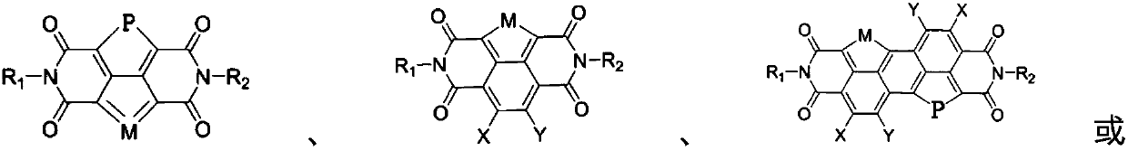
[0105] Embodiment 1 A kind of molecular structural formula is A method for preparing a semiconductor material, comprising the steps of:
[0106] a. Under nitrogen atmosphere, dissolve 30g of 1-bromo-3-fluoro-iodobenzene in 400ml of anhydrous ether, add 40ml of 2.5M n-butyllithium solution dropwise at -78°C, and then add 24g of copper bromide, stirred at low temperature for one hour, then added 14g of nitrobenzene, stirred overnight at room temperature, added water to quench the reaction, separated liquids, dried the organic phase with anhydrous sodium sulfate, rotary evaporated to remove the solvent, and purified through a column to obtain 7.83g molecular structure formula is White solid B1, yield 45%;
[0107] b. In a nitrogen atmosphere, dissolve 3.48g of compound B1 in 100ml of anhydrous toluene, add 3.4g of ethyl 3-mercaptoacrylate, 0.17g of tris(dibenzylideneacetone) dipalladium and 8.65g of anhydrous potassium carbonate, 110°C Heated for 20 hours, cooled, quenched w...
Embodiment 2
[0113] Embodiment 2 A kind of molecular structural formula is A method for preparing a semiconductor material, comprising the steps of:
[0114] a. Dissolve 17.4g chlorinated o-xylene in 250ml dichloromethane, add 0.5TMBAC, 50ml sodium sulfide nonahydrate (36g) solution is added dropwise in the dichloromethane solution, heat and reflux overnight, cool, wash with water, organic The phase was dried with anhydrous sodium sulfate, spin-dried, and purified by column chromatography to obtain 7.48g molecular structure formula: The transparent liquid B2, yield 55%;
[0115] b. Dissolve 5.44g of compound B2 in 100ml of chloroform, and add NaIO dropwise at 0°C 4 (8.56g) solution, stir overnight, remove inorganic salt by suction filtration, spin dry, recrystallize with ethyl acetate and sherwood oil, obtain 4.5g molecular structure formula is White solid C2, yield 75%;
[0116] c. Mix and grind 3g of compound C2 with 3g of neutral alumina powder, and sublimate to obtain 2.2g of mo...
Embodiment 3
[0120] Embodiment 3 A molecular structural formula is A method for preparing a semiconductor material, comprising the steps of:
[0121] a. Dissolve 17.1g of 3-bromo-o-dibromodibromotoluene in 200ml of DCM, add 0.5g of TEMBAC, and add 100ml (18g) of sodium sulfide nonahydrate solution dropwise, stir and reflux overnight, cool, wash with water, and separate the liquids. Drying over sodium sulfate, spin-drying, column chromatography purification, obtain 6.1g molecular structure formula is White solid B3, yield 57%;
[0122] b. Under nitrogen atmosphere, 0.6gNiCl 2 Add 1.45g of 2,2'-bipyridyl into 15ml of anhydrous DMF, heat to 70°C, after 20 minutes, add 10ml of B3 (1g) DMF solution dropwise, stir at 70°C for 12 hours, cool, and distill under reduced pressure DMF was removed, the solid was washed with water, extracted with DCM, the organic phase was dried over anhydrous sodium sulfate, concentrated and purified to obtain 0.26g of molecular structure formula: Yellow solid ...
PUM
 Abstract
Description
Claims
Application Information