Central processing unit design method supporting software code data confidentiality and credibility execution
A technology of central processing unit and design method, applied in the direction of electrical digital data processing, digital data protection, internal/peripheral computer component protection, etc.
- Summary
- Abstract
- Description
- Claims
- Application Information
AI Technical Summary
Problems solved by technology
Method used
Image
Examples
Embodiment 1
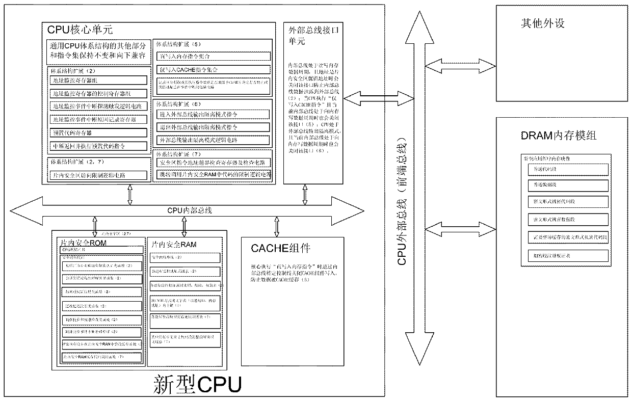
[0023] See attached figure 1 , assuming that the original CPU architecture has 32-bit address lines, the physical address space range is 0x00000000~0xFFFFFFFF, each physical address stores data in Byte (8bit) units, and the total address space is 4GByte. Expand the CPU In the new CPU architecture, the 512MByte address space of 0xE0000000~0xFFFFFFFF in the address space is set as the on-chip security area reserved address space, among which the 128M Byte address space of 0xF8000000~0xFFFFFFFF is allocated to the on-chip security ROM, and the 384M Byte of 0xE0000000~0xF7FFFFFF is allocated For the on-chip security RAM, 128M Byte OPTROM is integrated inside the CPU, and the address space is 0xF8000000~0xFFFFFFFF. This is the on-chip security ROM in this example. Secure RAM. When the new CPU is packaged, the image file synthesized by the pre-prepared "secure kernel code" and "CPU built-in private key certificate library" is written into the OPTROM packaged on-chip at one time. W...
Embodiment 2
[0041] This example continues to add logic circuits on the basis of the new CPU structure in Example 1, so as to make full use of the internal cache of the CPU, reduce the frequency of repeated decryption of encrypted segment data, and improve efficiency. The specific implementation method of this example is as follows:
[0042] In this example, the CPU's internal CACHE is connected to the CPU core with a Look-aside structure. In this example, the CPU uses the Write-through mode to write back data to the memory. Two control lines are added to the CPU's internal bus, one is called "CACHE shutdown control line", The control line is connected to the on-chip CACHE "chip select interface" through a logic circuit. When the control line outputs 1 (high level signal), the internal CACHE unit is closed; one is called the "external bus shutdown control line", and the control line passes through The logic circuit is connected with the "chip select interface" of the "CPU external interfac...
Embodiment 3
[0047] This example is different from Embodiments 1 and 2 without using the "address monitoring event interruption mechanism" and using another method "decryption cache mechanism for the entire encrypted segment" described in the present invention to realize. The specific implementation method of this example is as follows:
[0048] This example continues the setting of Example 1 and integrates 128M Byte OPTROM inside the CPU with an address space of 0xF8000000~0xFFFFFFFF as an on-chip security ROM; integrates an SRAM with an address space of 0xE0000000~0xF7FFFFFF inside the CPU as an on-chip security RAM. 0xE0000000~0xFFFFFFFF 512M Byte address space is reserved for the on-chip security area. Implement the "on-chip security area access restriction" in the same way as in Embodiment 1, that is, only the instruction code within the address range of 0xE0000000~0xFFFFFFFF can read and write the data within the address range of 0xE0000000~0xFFFFFFFF, and the data within the address...
PUM
 Abstract
Description
Claims
Application Information
