Control method for suppressing switching oscillation of field-effect transistor and second-order mode

A technology of field effect transistors and second-order models, applied in the direction of high-efficiency power electronic conversion, output power conversion devices, electrical components, etc., can solve problems such as oscillation and damage to electronic devices, and achieve the effect of high efficiency and suppression control methods

Active Publication Date: 2020-02-07
ELECTRIC POWER RESEARCH INSTITUTE, CHINA SOUTHERN POWER GRID CO LTD +1
View PDF4 Cites 2 Cited by
  • Summary
  • Abstract
  • Description
  • Claims
  • Application Information

AI Technical Summary

Problems solved by technology

[0009] The invention provides a control method and a second-order model for suppressing switching oscillations of field effect transistors, which are used to solve the technology that the existing silicon carbide MOSFET switching transient process has oscillations that may cause overvoltage and electromagnetic interference to damage electronic devices question

Method used


Image

  • Control method for suppressing switching oscillation of field-effect transistor and second-order mode
  • Control method for suppressing switching oscillation of field-effect transistor and second-order mode
  • Control method for suppressing switching oscillation of field-effect transistor and second-order mode

Examples


Embodiment 1

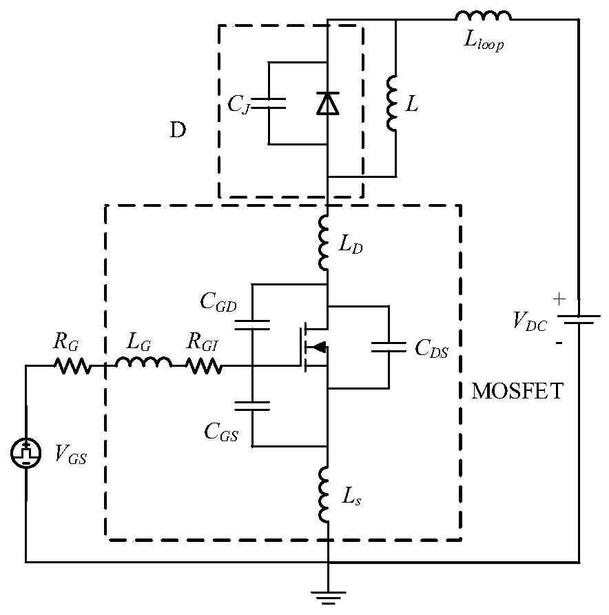
[0051] The typical double-pulse test circuit of the field effect transistor switching loop in the embodiment of the present invention is applied to a silicon carbide MOSFET, such as figure 1 as shown, figure 1 It is a typical double-pulse test circuit diagram of an existing field effect transistor switch circuit.

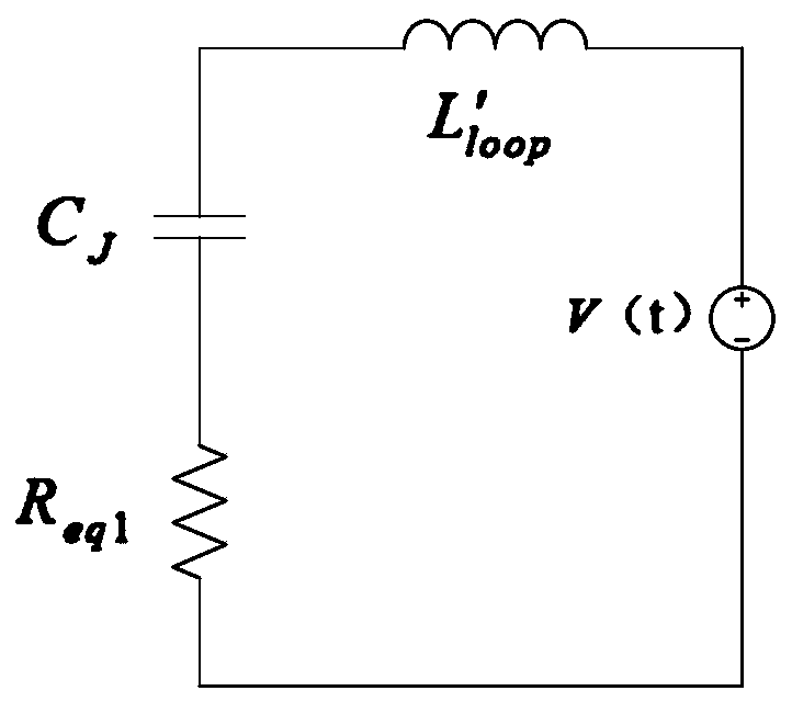
[0052] The field effect transistor switching loop includes a first power supply V DC , and the first power supply V DC The parasitic inductance L of the positive connection loop , and parasitic inductance L loop The connected diode D, the field effect transistor MOSFET connected to the anode of the diode D, and the drive resistor R connected to the gate of the field effect transistor MOSFET G and with drive resistor R G Connect the driver power supply V GS , drive power V GS with the first power supply V DC The negative pole of the diode D is connected in parallel with the first capacitor C J .

[0053] The gate of the field effect transistor MOSFET and th...

Embodiment 2

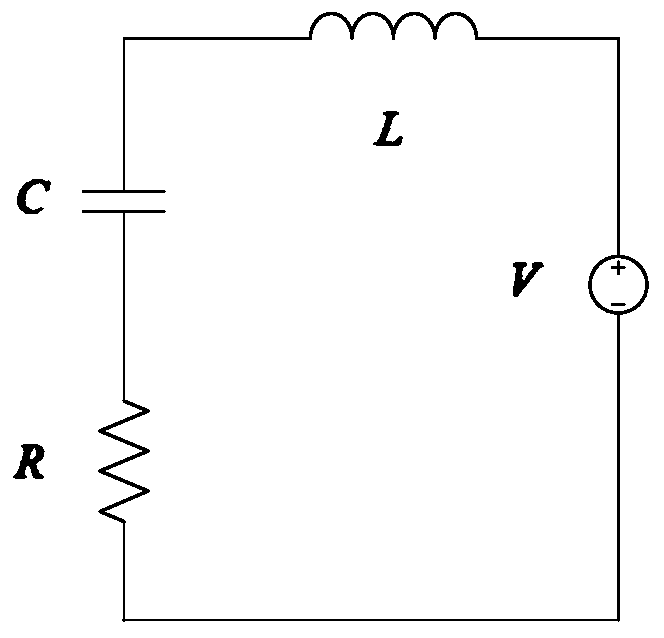
[0100] In addition, due to the high switching speed requirements of the field effect transistor application, the time requirement for the field effect transistor to be turned on or off, so according to the damping coefficient ξ 1 or / and ξ 2 Adjust the drive resistor R G . Such as Figure 5 as shown, Figure 5 It is a flow chart of the steps of the control method for suppressing the switching oscillation of the field effect transistor described in the embodiment of the present invention. The invention provides a control method for suppressing switching oscillation of a field effect transistor, comprising the following steps:

[0101] S1. Obtain the second-order model of the field effect transistor switching circuit;

[0102] S2. According to the second-order model, obtain the damping coefficient with the least time required in the turn-on and turn-off process in the second-order model of the field effect transistor switch circuit;

[0103] S3. Comparing the obtained dampi...


PUM


Abstract

The embodiment of the invention relates to a control method for suppressing switching oscillation of a field-effect transistor and a second-order model. The second-order model comprises a step power supply, a main loop inductor connected with the positive electrode of the step power supply, a main loop capacitor connected with the main loop inductor and a main loop resistor connected with the mainloop capacitor, wherein the main loop resistor is connected with the negative electrode of the step power supply. According to the control method for suppressing the switching oscillation of the field-effect transistor, through the second-order model of a switching loop of the field-effect transistor, the switching loop of the field-effect transistor does not need to connect additional damping equipment in a main loop in the switching loop of the field-effect transistor, and a new oscillation mode is not introduced; and by switching on and switching off the second-order model, driving resistance capable of suppressing oscillation in the switching-on or switching-off process of the field-effect transistor is obtained, so that oscillation in the switching-on or switching-off process of thefield-effect transistor is effectively suppressed, and the technical problem that oscillation occurs in the switch transient process of an existing silicon carbide MOSFET is solved.

Description

technical field [0001] The invention relates to the technical field of switching device oscillation, in particular to a control method for suppressing switching oscillation of a field effect transistor and a second-order model thereof. Background technique [0002] Wide bandgap semiconductor (third-generation semiconductor) devices represented by silicon carbide (SiC) and gallium nitride (GaN) have the characteristics of high junction temperature, high blocking voltage, and high switching frequency. It has the incomparable advantages of silicon-based devices. Silicon carbide-based MOSFET devices are currently a hot spot in research and application in the field of power electronics technology. [0003] Compared with the silicon-based IGBT that has been maturely applied, the switching speed of silicon carbide MOSFET is faster, the switching time is shorter, and it has the advantages of high frequency and low switching loss. However, due to the high voltage change rate dv / dt ...

Claims


Application Information

Patent Timeline
Patent Type & Authority Applications(China)
IPC IPC(8): H02M1/08
CPCH02M1/08H02M1/0038Y02B70/10
Inventor 喻松涛李巍巍
Owner ELECTRIC POWER RESEARCH INSTITUTE, CHINA SOUTHERN POWER GRID CO LTD
Why Eureka
Try Eureka