IGBT and manufacturing method thereof

An ion and target area technology, applied in electrical components, transistors, circuits, etc., can solve the physical properties of limited element boron, limit the further improvement of IGBT performance, etc. The effect of improving performance

Active Publication Date: 2020-03-03
ADVANCED SEMICON MFG CO LTD
View PDF2 Cites 3 Cited by
  • Summary
  • Abstract
  • Description
  • Claims
  • Application Information

AI Technical Summary

Problems solved by technology

[0003] However, in the current IGBT, limited by the physical properties of the element boron, the PN junction formed by the diffusion of boron ions is an abrupt junction, and the PN junction is related to the breakdown voltage, turn-off time and other properties, and further, the abrupt PN junction Junction limits further improvement of current IGBT performance

Method used


Image

  • IGBT and manufacturing method thereof
  • IGBT and manufacturing method thereof
  • IGBT and manufacturing method thereof

Examples


Embodiment 1

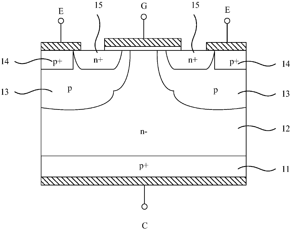
[0028] This embodiment provides an IGBT, figure 1 A schematic structural diagram of this embodiment is shown. see figure 1 , the IGBT of this embodiment includes from bottom to top:

[0029] The collector electrode C on the back of the IGBT, the P-type substrate 11, the N-type drift region 12, the P-type well region 13 located at both ends of the N-type drift region 12, the P-type source region 14 above the P-type well region 13, and the N-type Source region 15 , emitter E located above P-type source region 14 and part of N-type source region 15 , gate G located above part of N-type source region 15 , part of P-type well region 13 and part of N-type drift region 12 .

[0030] In the IGBT of this embodiment, the target region includes at least one of the P-type substrate 11, the P-type well region 13, and the P-type source region 14. In this embodiment, the doping impurities in the target region have a diffusion coefficient greater than that of boron ions. The first ions, sp...

Embodiment 2

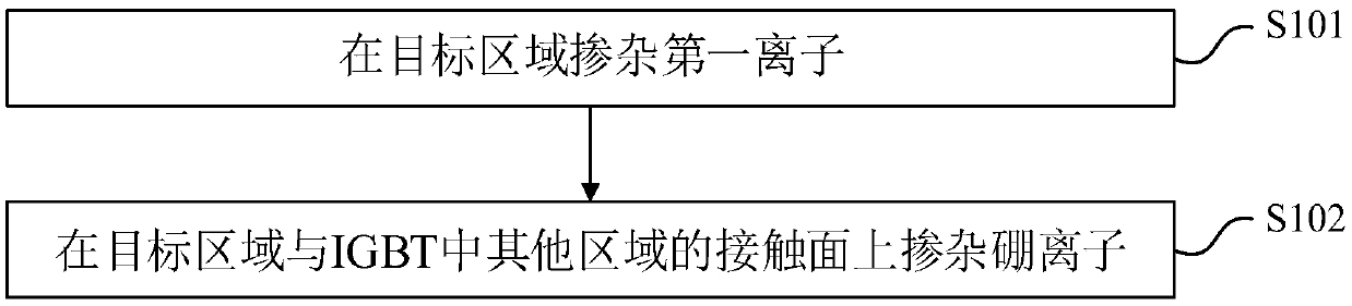
[0035] This embodiment provides a method for manufacturing an IGBT, which is used to manufacture the IGBT of Embodiment 1, figure 2 A flowchart of this embodiment is shown. see figure 2 , the method of this embodiment includes:

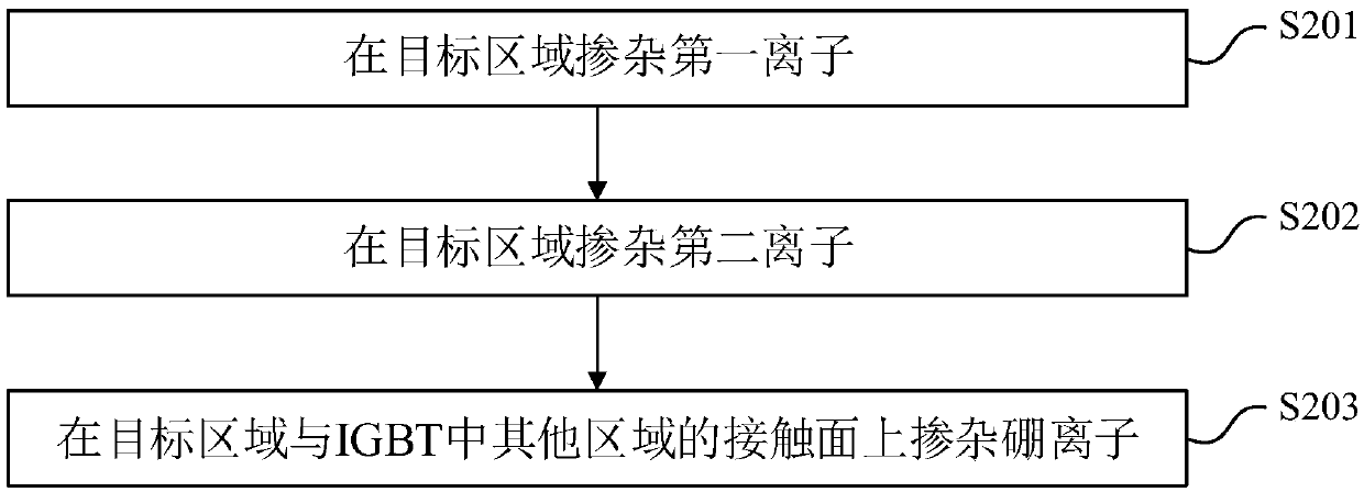
[0036] S101. Doping first ions in the target region;

[0037] S102 , doping boron ions on the contact surface between the target region and other regions in the IGBT.

[0038] Therefore, according to the selection of the target region in Embodiment 1, to specifically form the corresponding P-type substrate 11, P-type well region 13, and P-type source region 14, wherein, the first ions can be obtained through, but not limited to, ion implantation, diffusion, and evaporation. , Sputtering in any way to dope into the target area. In addition, boron ions can also be doped to a specific contact surface via but not limited to the above-mentioned methods, so as to avoid metal contamination caused by doped metal ions.

Embodiment 3

[0040] This embodiment provides an IGBT on the basis of Embodiment 1. Specifically, the improvement of the IGBT of this embodiment compared with Embodiment 1 lies in that the target region of this embodiment, that is, at least one of the P-type substrate 11, the P-type well region 13, and the P-type source region 14 , in addition to being doped with first ions, also doped with second ions, the diffusion coefficient of the second ions is not less than the diffusion coefficient of boron ions, specifically, the second ions can be but not limited to boron ions, aluminum ions , gallium ions, indium ions, thallium ions.

[0041] In this embodiment, the first ion is preferably aluminum ion, and the second ion is preferably gallium ion, or, the first ion is preferably gallium ion, and the second ion is preferably aluminum ion. In addition, the first ions and the second ions can be doped with each other or distributed in different layers according to specific applications. The doping...


PUM


Abstract

The invention discloses an IGBT and a manufacturing method thereof. A target region in the IGBT is doped with first ions, the target region comprises at least one of a P-type substrate, a P-type wellregion and a P-type source region, and the diffusion coefficient of the first ions is greater than that of boron ions. The diffusion coefficient of the first ions doped in the IGBT target region is greater than the diffusion coefficient of boron ions. Unlike the prior art of adopting boron ions as doping impurities, the distribution morphology of the impurities formed under the same condition is thus more gradually changed, that is, the formed PN junctions are gradually-changed junctions, so that the breakdown voltage is improved, the turn-off time is shortened, the latch-up resistance is improved, and the performance of the IGBT is further improved. Besides, the impurity diffusion coefficient is large, so that a wider and deeper PN junction can be formed at a lower temperature in a shorter time, and a certain cost advantage is achieved.

Description

technical field [0001] The invention relates to the technical field of semiconductors, in particular to an IGBT and a manufacturing method thereof. Background technique [0002] IGBT (Insulated Gate Bipolar Transistor, Insulated Gate Bipolar Transistor) combines the advantages of BJT (Bipolar Junction Transistor, Bipolar Transistor) and power MOSFET (Metal-Oxide-Semiconductor Field-Effect Transistor, Metal-Oxide-Semiconductor Field-Effect Transistor) , has the advantages of both high input impedance and low conduction voltage drop, and is widely used in various power integrated circuit fields. [0003] However, in the current IGBT, limited by the physical properties of the element boron, the PN junction formed by the diffusion of boron ions is an abrupt junction, and the PN junction is related to the breakdown voltage, turn-off time and other properties, and further, the abrupt PN junction The junction limits the further improvement of current IGBT performance. Contents o...

Claims


Application Information

Patent Timeline
Patent Type & Authority Applications(China)
IPC IPC(8): H01L29/739H01L29/167
CPCH01L29/167H01L29/7398H01L29/7395H01L29/1095H01L29/66333H01L29/0834H01L29/0611H01L29/66325H01L29/7393
Inventor 王学良刘建华郎金荣闵亚能
Owner ADVANCED SEMICON MFG CO LTD
Why Eureka
Try Eureka