High-voltage terahertz strained sige/ingap heterojunction bipolar transistor and its preparation method

A heterojunction bipolar and terahertz technology, which is applied in semiconductor/solid-state device manufacturing, semiconductor devices, electrical components, etc., can solve problems such as reducing and limiting SiGe-HBT high-speed/high-power performance, and achieve improved interface characteristics, Effects of Improving Frequency and Power Characteristics

Active Publication Date: 2020-11-20
YANSHAN UNIV
View PDF4 Cites 0 Cited by
  • Summary
  • Abstract
  • Description
  • Claims
  • Application Information

AI Technical Summary

Problems solved by technology

Because the carrier transport time is determined by the saturation velocity of the carriers in the material, the increase of the electric field will cause the avalanche breakdown effect caused by the multiple impact ionization of the carriers in the collector area, and the avalanche multiplication factor depends largely on Due to the forbidden band width of the material, so in order to increase the cut-off frequency f of the device T , will make the common emitter collector junction avalanche breakdown voltage (BV CEO ) drops, thus limiting the high speed / high power performance of SiGe-HBT

Method used


Image

  • High-voltage terahertz strained sige/ingap heterojunction bipolar transistor and its preparation method
  • High-voltage terahertz strained sige/ingap heterojunction bipolar transistor and its preparation method
  • High-voltage terahertz strained sige/ingap heterojunction bipolar transistor and its preparation method

Examples


Embodiment Construction

[0045] Hereinafter, embodiments of the present invention will be described with reference to the drawings.

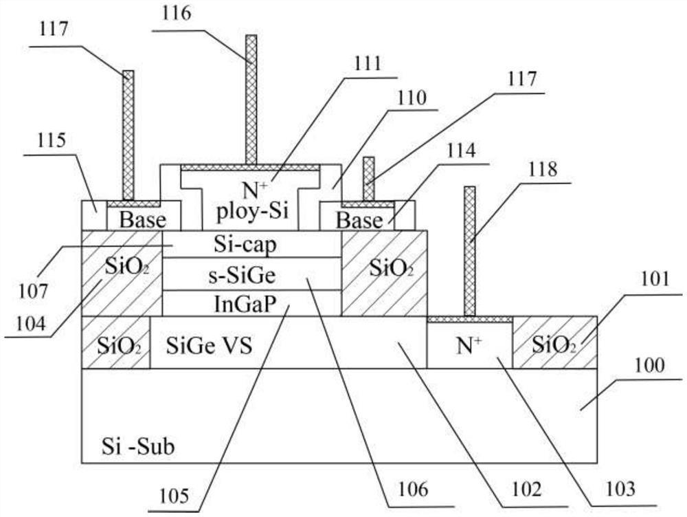
[0046] like figure 1 As shown, a kind of high-voltage terahertz strain SiGe / InGaP heterojunction bipolar transistor provided by the present invention, this bipolar transistor selects the N-type doped single crystal Si substrate that crystal direction is (001); On the substrate An epitaxial N-type SiGe layer with a Ge composition gradient is used as a sub-collector region, and N+ doping is performed on the right side; a thick layer of SiO is deposited on the surface of the SiGe layer. 2 layer to define the position of the active region; the MBE method is used to epitaxially N-type InGaP layer, P-type SiGe layer and intrinsic Si cap layer in the active region; nitride and oxide layers and side wall oxide layers are deposited on the device surface , deposit polysilicon on the sidewall oxide layer as the emitter; etch the nitride, and then selectively epitaxial polysilicon...


PUM


Abstract

The invention provides a high-voltage terahertz strain SiGe / InGaP heterojunction bipolar transistor and a preparation method thereof. The InGaP material has the high carrier mobility of the InP material and the wide band gap of the GaP material. Therefore, the present invention uses InGaP as the collector region, which can improve the frequency and power characteristics of the device at the same time, so that the device can realize the terahertz frequency band. The system integration of the chip, further the present invention utilizes the advantage of "energy band engineering", adopts In 1‑x Ga x P (x = 0 ~ 1) is used as the collector material of SiGe-HBT, and the molar ratio x of In and Ga is properly selected so that it has the same lattice constant as the sub-collector material SiGe, which can effectively Improve the interface properties of InGaP and SiGe materials.

Description

technical field [0001] The invention relates to the technical field of semiconductor integrated circuits, in particular to a high-voltage terahertz strained SiGe / InGaP heterojunction bipolar transistor and a preparation method thereof. Background technique [0002] Integrated circuits have developed into the 10nm era, and the feature size of devices has been further reduced. Therefore, it is necessary to seek breakthroughs in basic fields such as device physics, materials, device structures, key processes, and integration technologies. At the same time, silicon-based circuits have entered the field of terahertz wave applications, and the requirements for high performance and low power consumption of SiGe BiCMOS (silicon germanium bipolar CMOS) are also getting higher and higher. [0003] SiGe heterojunction bipolar transistor (HBT) is a Si-based bipolar junction transistor (BJT) base region added a small amount of Ge components. The use of SiGe material in the base region s...

Claims


Application Information

Patent Timeline
Patent Type & Authority Patents(China)
IPC IPC(8): H01L29/737H01L29/267H01L21/331
CPCH01L29/267H01L29/66318H01L29/7371H01L29/0821H01L29/1004H01L29/0817H01L29/737
Inventor 周春宇李洪岩耿欣王冠宇蒋巍乔世峰耿连民
Owner YANSHAN UNIV
Why Eureka
Try Eureka