Deep hole superlattice filling method based on electrochemical deposition

A filling method, electrochemical technology, applied in the direction of electrical components, nanotechnology, etc., can solve problems such as filling method blockage, and achieve the effects of avoiding reaction interruption, simple and easy operation, and low energy consumption

Active Publication Date: 2020-03-24
HUAZHONG UNIV OF SCI & TECH
View PDF5 Cites 0 Cited by
  • Summary
  • Abstract
  • Description
  • Claims
  • Application Information

AI Technical Summary

Problems solved by technology

[0005] Aiming at at least one of the above defects or improvement needs of the prior art, especially the clogging problem existing in the existing filling method, the present invention provides a method for reusing deep holes with nanoscale apertures etched by micro-nano processing technology. The method of electrochemical deposition is a process method for quickly and effectively filling deep holes, which can grow nano-phase change materials from the bottom of nano-holes, and can realize ultra-large aspect ratio small holes for filling chalcogenide phase-change materials

Method used


Image

  • Deep hole superlattice filling method based on electrochemical deposition
  • Deep hole superlattice filling method based on electrochemical deposition
  • Deep hole superlattice filling method based on electrochemical deposition

Examples


specific Embodiment approach

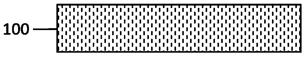
[0067] Place the silicon wafer in acetone and alcohol for ultrasonic cleaning for about ten minutes; after the ultrasonic is completed, use a nitrogen gun to blow off the residual liquid on the surface and dry it for use.

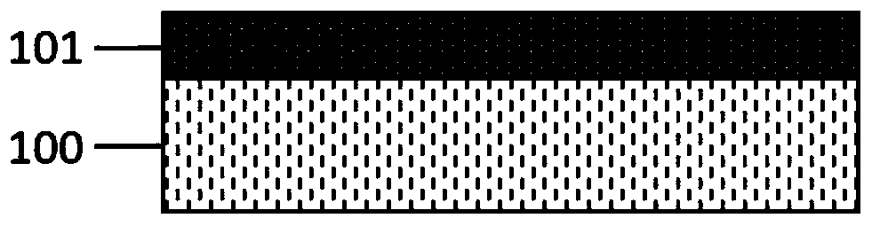
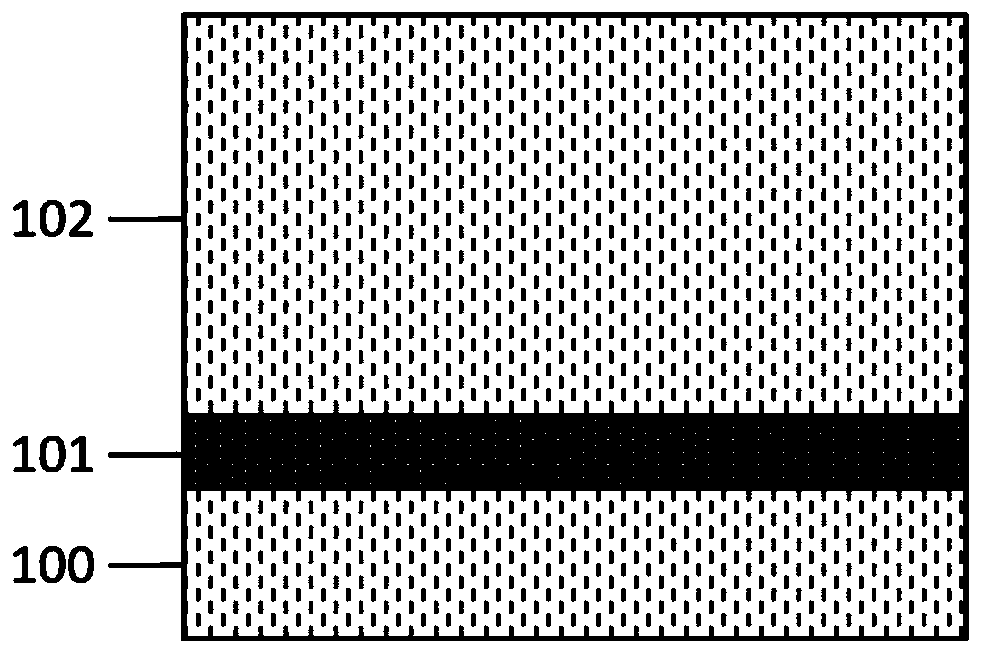
[0068] Use magnetron sputtering or electron beam evaporation to evaporate a metal conductive layer such as titanium platinum, nickel gold, etc. on a clean silicon wafer, with a thickness between 10nm and 200nm. Use PECVD or ALD to grow a layer of dense silicon dioxide or alumina. This step involves a high reaction temperature, but there is no functional layer on the sample, which will not affect the performance of the device. The thickness can reach the micron level or more according to the design requirements.

[0069] Combined with photolithography or other mask processes, the pattern is transferred to the sample. Use the etching method to etch small holes. If the depth of subsequent etching is deeper, the mask can be replaced with a mask that is more re...


PUM

PropertyMeasurementUnit
pore sizeaaaaaaaaaa
thicknessaaaaaaaaaa
thicknessaaaaaaaaaa

Abstract

The invention discloses a deep hole superlattice filling method based on electrochemical deposition. The method comprises the following steps: S1, preparing a conductive substrate; S2, preparing an insulating layer; S3, preparing a deep hole; S4, preparing a reaction solution, wherein two different electrolytes are mixed in the reaction solution; S5, carrying out the electrochemical deposition inthe deep hole from bottom to top, adjusting the deposition parameters, alternately depositing a first phase change material layer and a second phase change material layer in the deep hole, and forminga superlattice structure; S6, preparing an upper electrode. According to the method, the deep hole with the nanoscale aperture is etched through the micro-nano machining technology, and then the electrochemical deposition method is used for quickly and effectively filling the deep hole; the nano phase-change material can grow from the bottom of the nano hole, the sulfur phase-change material canbe filled in the small hole with the ultra-large depth-to-width ratio, and the growth of the material can be accurately regulated and controlled by regulating and controlling deposition parameters.

Description

technical field [0001] The invention belongs to the technical field of microelectronic devices and memories, and in particular relates to a deep hole superlattice filling method based on electrochemical deposition. Background technique [0002] The traditional phase-change memory (PCM) has gradually been unable to meet the demand for high-capacity storage in the era of big data. Whether it is the three-dimensional stacking of PCM or the continuous reduction of device size, it is to improve storage density and reliability. However, with the advancement of process nodes, not only the increasing aspect ratio of the device structure makes it difficult to fill deep holes in the process, but also large-scale integration needs to rely on fast and effective deep hole filling processes. [0003] Although advanced photolithography processes can carve nano-aperture patterns, commonly used dry etching processes such as plasma etching, ion beam etching, and reactive ion etching methods c...

Claims


Application Information

Patent Timeline
Patent Type & Authority Applications(China)
IPC IPC(8): H01L45/00B82Y40/00
CPCB82Y40/00H10N70/023H10N70/066
Inventor 童浩万代兴缪向水徐开朗
Owner HUAZHONG UNIV OF SCI & TECH
Why Eureka
Try Eureka