Photoelectric device based on graphene/tungsten diselenide/tin diselenide laminated structure and preparation method thereof
A technology of tungsten diselenide and tin diselenide, which is applied in the direction of electrical components, semiconductor devices, circuits, etc., can solve the problems of reducing photocurrent and not fully meeting the responsivity requirements of optoelectronic devices, and achieve high photoresponsivity and sensitivity , excellent ohmic contact characteristics, simple preparation process
- Summary
- Abstract
- Description
- Claims
- Application Information
AI Technical Summary
Problems solved by technology
Method used
Image
Examples
Embodiment 1
[0039] 1. Prepare photodetectors, the specific preparation steps are as follows:
[0040] 1) Substrate cleaning
[0041] Soak the silicon oxide-silicon substrate to be cleaned in acetone solution, isopropanone, and absolute ethanol for 5 minutes and ultrasonically clean it at 20KHz for 10 minutes. After cleaning, rinse it with deionized water, dry it with nitrogen gas, and set it aside.
[0042] 2) Preparation of layered materials
[0043] In this example, the three layered materials were prepared by mechanical exfoliation. The tungsten diselenide, tin diselenide and graphene layered materials to be peeled off are placed on the adhesive tape respectively, and the block material is pasted and peeled off repeatedly, so that it becomes a thinner layered sheet. The layered flakes on the tape were pasted on the silicon oxide-silicon substrate, compacted repeatedly, and the tape was slowly peeled off after standing for 5 minutes, so that the materials remained on the substrate, th...
Embodiment 2
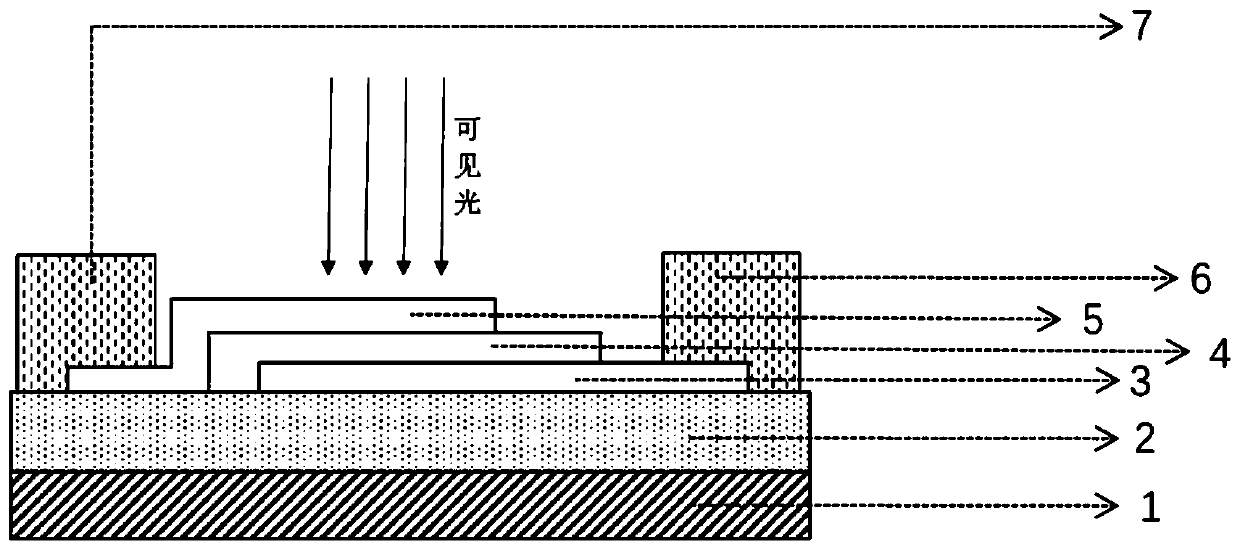
[0057] The difference between this embodiment and Embodiment 1 is that the quartz glass 1 with a thickness of 0.6 mm is selected as the substrate, and the surface is covered with a boron nitride layer 2 with a thickness of 120 nm. On the boron nitride layer, a tin diselenide layer 3 with a thickness of 10 nanometers, a tungsten diselenide layer 4 with a thickness of 20 nanometers, and a graphene layer 5 with a thickness of 0.7 nanometers are stacked from bottom to top. The first metal electrode 6 and the second The metal electrode 7 is a gold electrode added with indium gallium alloy.
[0058] In this embodiment, a boron nitride layer with a thickness of 120 nm is stacked on a quartz substrate with a thickness of 0.6 mm to form the insulating layer 2 by using a mechanical transfer method. Electrodes were prepared by vapor-depositing InGa-metal alloys. That is, in an evaporation apparatus, the indium-gallium-metal alloy is used as the target material, and the indium-gallium-me...
Embodiment 3
[0064] In this embodiment, the difference from Embodiment 2 is that the mica with a thickness of 1 mm is selected as the substrate 1. Since the mica is an insulating substrate, the substrate 1 and the insulating layer 2 are solidly integrated in this embodiment. Made of mica. A tin diselenide layer 3 with a thickness of 8 nm, a tungsten diselenide layer 4 with a thickness of 17 nm, and a graphene layer 5 with a thickness of 1 nm are sequentially stacked on the substrate 1 / insulating layer 2 from bottom to top. The first metal electrode 6 and the second metal electrode 7 are indium gallium alloy, and its structure is as follows Figure 4 shown.
[0065] In this embodiment, the layered material and laminated structure are prepared by mechanical stripping method and mechanical transfer method respectively, and the first metal electrode 6 and the second metal electrode 7 are prepared by brushing liquid indium gallium alloy. The implementation steps are the same as in Example 1. ...
PUM
| Property | Measurement | Unit |
|---|---|---|
| thickness | aaaaa | aaaaa |
| thickness | aaaaa | aaaaa |
| thickness | aaaaa | aaaaa |
Abstract
Description
Claims
Application Information


