
Photoinduced field emission cathode electron emission device

A cathode electron emission and field emission technology, which is applied in the direction of photoemission cathodes, circuits, electrical components, etc., can solve the problems of high electric field and high power supply requirements, and achieve the effect of increasing current density, excellent electron emission characteristics, and reducing requirements

Pending Publication Date: 2020-05-26
SOUTHWESTERN INST OF PHYSICS +1
View PDF0 Cites 0 Cited by
  • Summary
  • Abstract
  • Description
  • Claims
  • Application Information

AI Technical Summary

Problems solved by technology

The problem is that the electric field of field emission is too high, and the requirements for the corresponding power supply are high.

Method used


Image

  • Photoinduced field emission cathode electron emission device
  • Photoinduced field emission cathode electron emission device
  • Photoinduced field emission cathode electron emission device

Examples


Embodiment Construction

[0022] The present invention will be described in further detail below in conjunction with the accompanying drawings and specific embodiments.

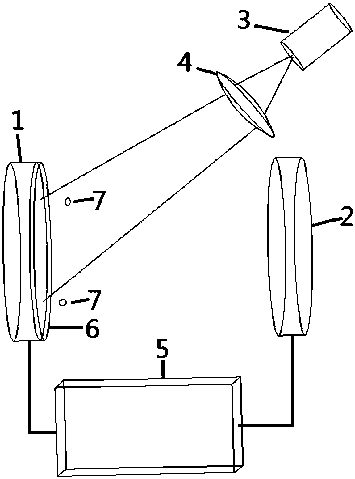
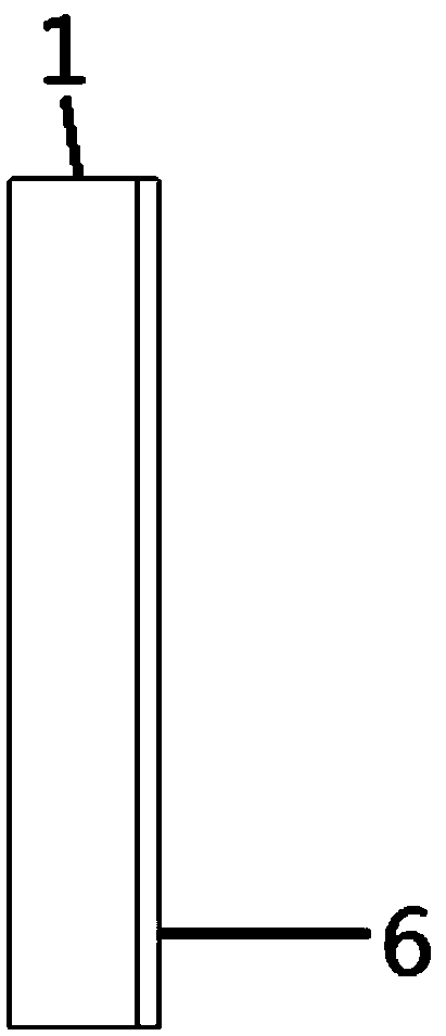
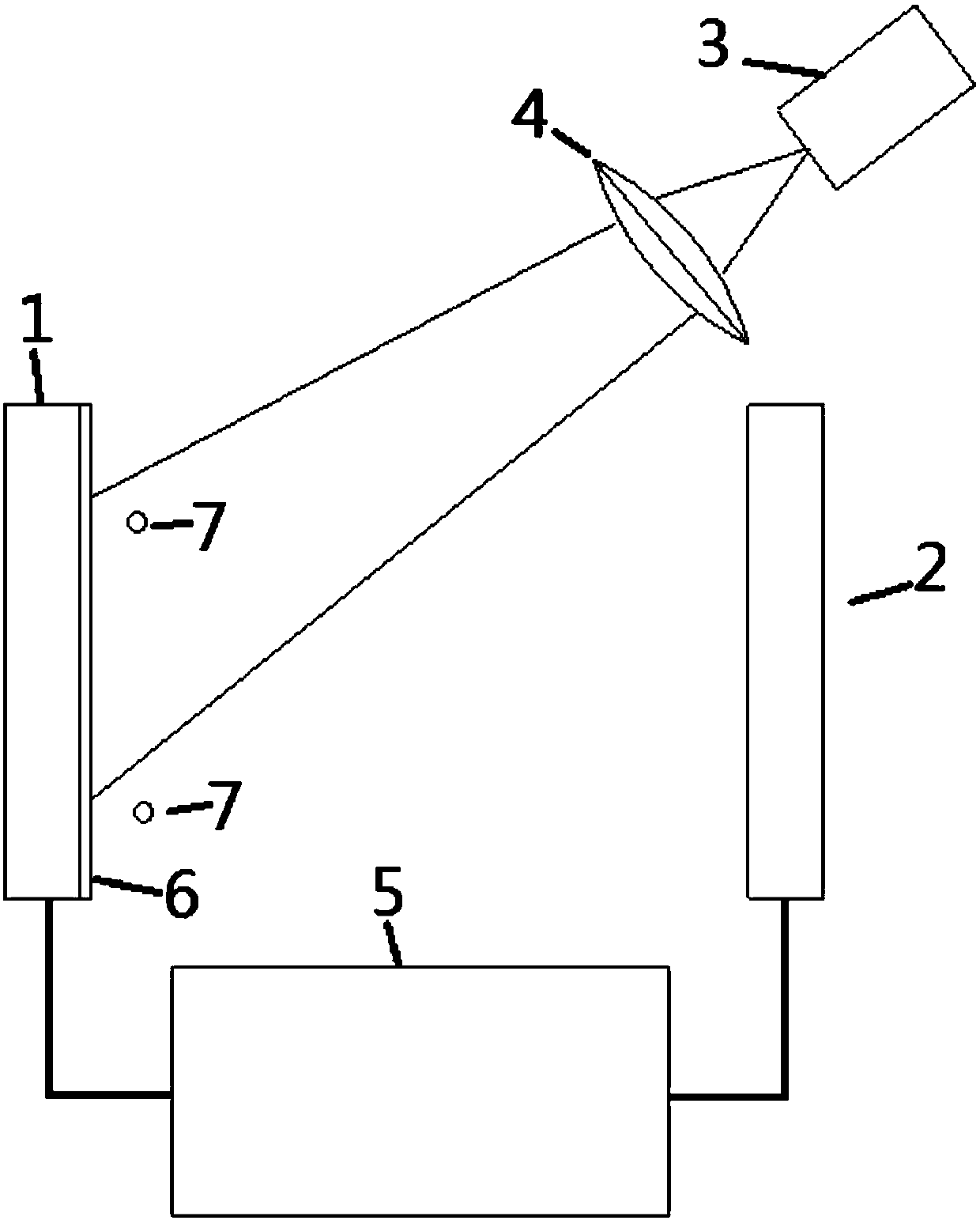
[0023] Such as figure 1 As shown, a light-induced field emission cathode electron emission device of the present invention is composed of a cathode 1, an anode 2, a light-emitting device 3, an optical component 4, and a DC high-voltage power supply 5. The cathode and the anode are cylindrical, and the edges of the opposite surface of the cathode and the anode are rounded with a certain radius to avoid field strength enhancement caused by the geometry; the distance between the cathode and the anode is on the order of millimeters.

[0024] Such as figure 1 As shown, the light emitting device 3 can be a light emitting diode LED or a semiconductor laser LD. The light-emitting device 3 is a monochromatic visible light or an infrared light-emitting diode LED or a semiconductor laser LD. It is very important to select the wavelength of lig...


PUM


Abstract

The invention relates to the field of electron emission devices, and particularly relates to a photoinduced field emission cathode electron emission device. The device comprises a cathode, an anode, alight emitting device, an optical assembly and a direct-current high-voltage power supply, wherein the cathode and the anode are connected to the direct-current high-voltage power supply; the cathodeand the anode are parallel and perpendicular to the horizontal line, the surface of the cathode is covered with a thin film material, and under the action of monochromatic light, electrons in the surface of a thin film material on the cathode obtain photon energy to generate free carrier absorption or lattice absorption or exciton absorption to generate high-energy electrons. According to the device, the current density of emission electrons of a field emission cathode electron source is effectively improved on the basis of not influencing the miniaturization of the cathode electron emissiondevice, the requirement of field emission electron emission for a power supply is effectively reduced at the same time, the combination of excellent electron emission characteristics and excellent conductivity of the surface can be achieved, and then excellent field emission characteristics are obtained.

Description

technical field [0001] The invention relates to the field of electron emission devices, in particular to a light-induced field emission cathode electron emission device. Background technique [0002] Thermionic emission is the most widely used and most mature electron emission method in the field of solid surface electron emission. Thermionic emission type, that is: using a hot filament cathode, under the action of an independent heating source, some electrons in the metal surpass the surface barrier and escape from the surface to achieve electron emission. Thermionic emission is widely used in CRT display, industrial production, medical treatment and other fields. However, thermionic emission has problems such as large volume, the need for an additional independent cathode power supply, slow frequency response, large heat generation, and the need for refrigeration. In some applications, such as the miniaturization of X-ray tubes, thermionic emission is difficult to adapt ...

Claims


Application Information

Patent Timeline
IPC IPC(8): H01J1/304H01J1/34
CPCH01J1/304H01J1/34
Inventor 李建童洪辉王坤但敏金凡亚
Owner SOUTHWESTERN INST OF PHYSICS
Learn More