

P-type semiconductor low-resistance ohmic contact structure and preparation method thereof
An ohmic contact and semiconductor technology, which is applied in semiconductor/solid-state device manufacturing, semiconductor devices, electrical components, etc., can solve the problems of P-GaN heavy doping difficulty, poor stability, and large contact resistance, so as to simplify the process flow and improve Thermal stability, the effect of avoiding damage to the device
- Summary
- Abstract
- Description
- Claims
- Application Information
AI Technical Summary
Problems solved by technology
Method used
Image

Examples
preparation example Construction
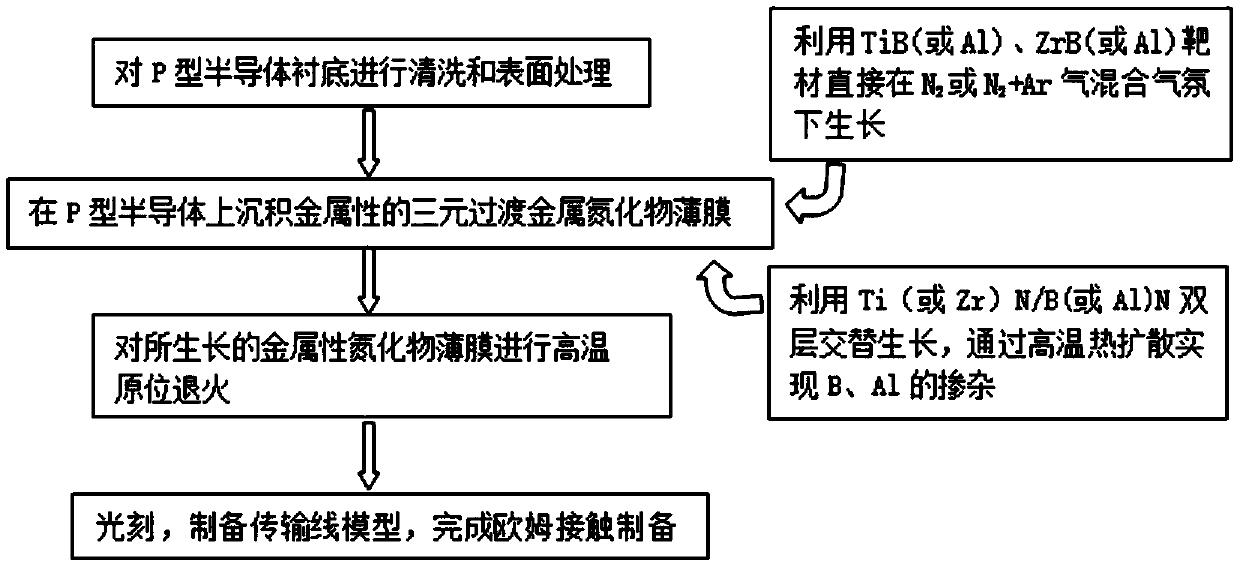
[0019] The embodiment of the present invention also provides a method for preparing a P-type semiconductor low-resistance ohmic contact structure, which includes: growing a metallic ternary transition metal nitride film on a P-type semiconductor substrate, and controlling the formed ternary transition metal nitride film. The metal nitride thin film is subjected to in-situ annealing treatment; wherein, the material of the ternary transition metal nitride thin film includes any one or a combination of TiBN, ZrBN, TiAlN, and ZrAlN.
[0020] In some more specific embodiments, the preparation method includes: firstly cleaning and surface-treating the P-type semiconductor substrate, and then growing the ternary transition metal nitride thin film on the surface of the P-type semiconductor substrate. The above mentioned surface treatment includes Ar plasma treatment.
[0021] In some more specific embodiments, the preparation method includes: using pulsed laser deposition technology, ...
Embodiment 1
[0048] The present invention provides a kind of preparation method of P-type semiconductor ohmic contact, and its specific steps are as follows:
[0049] Step 1: Using P-GaN material with a hole concentration of 6×10^(16)cm^(-3), ultrasonically clean the P-GaN substrate with acetone, ethanol, and deionized water for 5 minutes; use up N 2 Blow it dry and put it into the epitaxial growth chamber of the pulsed laser deposition system;
[0050] Step 2: The temperature of the substrate is raised to 650° C., and argon gas is introduced into the epitaxial growth chamber of the pulsed laser deposition system through the gas pipeline and the pressure is adjusted to 3 Pa. Argon gas is ionized by the discharge device of the pulsed laser system to generate argon plasma. Under the bombardment of argon plasma, the surface of the sample is treated to remove the oxide layer and other impurities on the surface;
[0051] Step 3: After 10 minutes of ionization, end the ionization and stop flo...
Embodiment 2
[0059] The present invention provides a kind of preparation method of P-type semiconductor ohmic contact, and its specific steps are as follows:
[0060] Step 1: Using P-GaN material with a hole concentration of 6×10^(16)cm^(-3), ultrasonically clean the P-GaN substrate with acetone, ethanol, and deionized water for 5 minutes; use up N 2 Blow it dry and put it into the epitaxial growth chamber of the pulsed laser deposition system;
[0061] Step 2: The temperature of the substrate is raised to 650° C., and argon gas is introduced into the epitaxial growth chamber of the pulsed laser deposition system through the gas pipeline and the pressure is adjusted to 3 Pa. Argon gas is ionized by the discharge device of the pulsed laser system to generate argon plasma. Under the bombardment of argon plasma, the surface of the sample is treated to remove the oxide layer and other impurities on the surface;
[0062] Step 3: After 10 minutes, end the ionization and stop flowing argon. I...
PUM
| Property | Measurement | Unit |
|---|---|---|
| Thickness | aaaaa | aaaaa |
| Work function | aaaaa | aaaaa |
| The inside diameter of | aaaaa | aaaaa |
Abstract
Description
Claims
Application Information