Supercharge Your Innovation With Domain-Expert AI Agents!

Wafer full laser dicing method

A cutting method and wafer technology, applied in the field of wafer processing, can solve the problems of inability to meet processing standards, low production efficiency, low dielectric constant, etc., to reduce thermal effects, reduce the loss of cutting grooves, and increase the number of chips Effect

Active Publication Date: 2020-09-08
佛山市联动科技股份有限公司
View PDF9 Cites 0 Cited by
  • Summary
  • Abstract
  • Description
  • Claims
  • Application Information

AI Technical Summary

Problems solved by technology

[0004] Moreover, with the background of high integration such as SiP (System in Package), high flexural strength sheet manufacturing technology is becoming more and more important, and wafers with a thickness of less than 100 μm will gradually become the mainstream. Blades cannot be directly used for cutting such thin wafers; and the low dielectric constant (Low-k) film and copper materials that are gradually adopted on high-speed electronic components are difficult to cut with ordinary diamond grinding wheel blades, sometimes It cannot meet the processing standards required by electronic component manufacturers. Compound semiconductors such as GaAs (gallium arsenide), GaN (gallium nitride), and GaP (gallium phosphide) used in high-frequency electronic components are cut with diamond grinding wheel blades. However, in the existing technology, although the laser cutting technology is used to replace the traditional diamond grinding wheel blade cutting, it still needs to be split after laser cutting in order to truly realize the cutting of the wafer. Segmentation, which improves the yield rate to a certain extent, but the efficiency is still not high

Method used


Image

  • Wafer full laser dicing method
  • Wafer full laser dicing method
  • Wafer full laser dicing method

Examples


Embodiment 1

[0023] Embodiment 1: a kind of laser full cutting method of wafer, comprises the following steps:

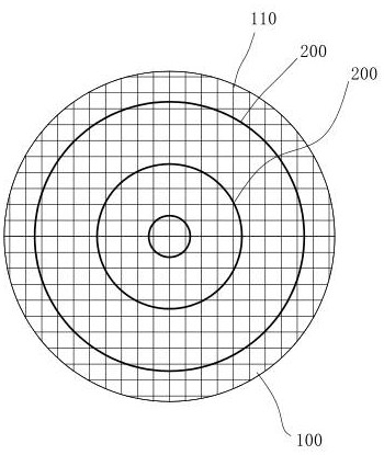
[0024] First, calibrate and measure the center of gravity of the wafer; then load the wafer; since the thinner the wafer, the easier it is to warp, and the center of gravity of the wafer will change after warping. Use the center of gravity to adjust the calibrator to confirm the center of gravity of the wafer. After confirming the center of gravity, send the wafer to the vacuum table with X, Y direction movement and rotation for vacuum adsorption through a fully automatic manipulator; in this step, by adding the link of center of gravity calibration It can ensure the accuracy of the placement position of the wafer on the vacuum suction table and the uniformity of adsorption, which is beneficial to reduce the fragmentation rate.

[0025] Then, after the wafer is absorbed and flattened, the X and Y of the platform are moved to the positioning calibration vision to detect and posit...


PUM

PropertyMeasurementUnit
thicknessaaaaaaaaaa

Abstract

The invention discloses a method for laser full cutting of a wafer, comprising the following steps: A. calibrating and measuring the center of gravity of the wafer; B. loading the wafer according to the center of gravity determined in step A; C. The adsorption position of the wafer is detected and positioned; D, the cooling liquid is evenly coated on the surface of the wafer; E, the laser is used to draw a cutting groove on the surface of the wafer, and the depth of the cutting groove is 10 μm ~ 15 μm; F 1. Homogenize the coolant on the surface of the wafer again; G. Adjust the parameters of the laser, and shape the laser beam at the same time, so that the laser beam has a blade, and use the blade to cut the wafer along the cutting groove. The beneficial effects of the present invention are: the present invention realizes the direct cutting of the wafer by adopting the laser full cutting mode, greatly reduces the problem of its fragmentation rate; greatly improves the production efficiency; increases the number of chips that can be produced in the wafer; reduces the laser The influence of the thermal effect brought by cutting.

Description

technical field [0001] The invention relates to a wafer processing method, in particular to a wafer laser cutting method. Background technique [0002] Wafers are widely used in the chip industry. During the processing of chips, wafers need to be divided. At present, the wafer segmentation method is realized by loading, cutting, cleaning / drying, and the cutting is achieved by single-spindle or opposed double-spindle, parallel double-spindle grinding wheel blades to groove and then cut, or The laser is used to slot first and then the grinding wheel blade to cut. But the whole cutting process is always inseparable from the diamond grinding wheel blade; as the size of the wafer develops from 4 inches, 6 inches, 8 inches to 12 inches, its size continues to increase, and the thickness correspondingly changes from the original 300μm, 200μm, From 150 μm to the current 100 μm and 75 μm, the thickness is constantly decreasing. [0003] However, for grinding wheel blade cutting, th...

Claims


Application Information

Patent Timeline
Patent Type & Authority Patents(China)
IPC IPC(8): H01L21/304H01L21/78B23K26/38B23K26/402B23K26/146B23K26/70B23K37/04
CPCB23K26/146B23K26/38B23K26/402B23K26/70B23K26/702B23K37/0408B23K2101/40
Inventor 何国洪
Owner 佛山市联动科技股份有限公司
Features
  • R&D
  • Intellectual Property
  • Life Sciences
  • Materials
  • Tech Scout
  • Unparalleled Data Quality
  • Higher Quality Content
  • 60% Fewer Hallucinations
Learn More