Gallium oxide semiconductor structure, solar-blind photodetector and preparation method

A photodetector, gallium oxide technology, applied in semiconductor devices, photovoltaic power generation, circuits, etc., can solve the problems of long switching time, failure to realize high-performance gallium oxide solar-blind photodetector preparation, and reduce detector responsivity

Active Publication Date: 2020-10-20
SHANGHAI INST OF MICROSYSTEM & INFORMATION TECH CHINESE ACAD OF SCI
View PDF9 Cites 2 Cited by
  • Summary
  • Abstract
  • Description
  • Claims
  • Application Information

AI Technical Summary

Problems solved by technology

At present, gallium oxide is difficult to achieve p-type doping, and it is still very difficult to heteroepitaxy high-quality gallium oxide thin films. However, gold-semi-gold photodetectors are simple to prepare, have high responsivity, and are compatible with modern CMOS processes. Therefore, gold-semi-gold photodetectors -Gold thin film detector is currently the most widely used form of gallium oxide solar blind detection
[0004] According to the current investigation and research, the bulk materials of gallium oxide are becoming more and more mature, and the preparation methods of thin film materials have also been developed. The commonly used epitaxy methods include MBE, MOCVD, PLD, etc., but the β-type gallium oxide (β-Ga 2 o 3 ) The quality of single crystal film depends on factors such as lattice matching, growth temperature, raw material supply, deposition rate and annealing temperature. To grow high-quality β-Ga 2 o 3 Single crystal thin films are difficult and have poor reproducibility, high cost and low efficiency
However, the quality of the single crystal thin film is the key factor to determine whether the performance of the photodetector is good, for example, β-Ga 2 o 3 Oxygen vacancy defects in the film act as trap centers to capture photogenerated carriers, which will lead to longer switching times, and structural dislocations as effective recombination centers will reduce the responsivity of the detector. In addition, extrinsic transitions caused by defects may Reduce the selectivity of the detector to the detection wavelength, affecting the detection of the sun-blind band
Therefore, it is extremely important to prepare high-quality gallium oxide thin films. However, the current preparation methods of thin films have not yet achieved the preparation of high-performance gallium oxide solar-blind photodetectors.
[0005] Based on this, the most critical issue is to prepare a gallium oxide film with the same quality as the bulk material. Transferring a single crystal gallium oxide film to a silicon (Si) heterogeneous substrate by ion beam exfoliation is currently the most important way to prepare a single crystal gallium oxide film. The best method for thin films, but there is leakage through the direct bonding of gallium oxide to the Si substrate, which affects the performance of the device. At the same time, gallium oxide and silicon oxide (SiO 2 ) bonding technology is not yet mature

Method used


Image

  • Gallium oxide semiconductor structure, solar-blind photodetector and preparation method
  • Gallium oxide semiconductor structure, solar-blind photodetector and preparation method
  • Gallium oxide semiconductor structure, solar-blind photodetector and preparation method

Examples


preparation example Construction

[0075] This embodiment also provides a method for preparing a solar-blind photodetector, comprising the following steps:

[0076] The gallium oxide semiconductor structure is prepared by the above preparation method of the gallium oxide semiconductor structure;

[0077] Fabricate interdigitated electrodes on the gallium oxide semiconductor structure.

[0078] As an example, the width of the interdigital electrodes is 2 μm to 500 μm, such as 50 μm, 100 μm, 200 μm, 300 μm, 400 μm, etc., and the length is 50 μm to 5000 μm, such as 100 μm, 500 μm, 1000 μm, 3000 μm, etc. The distance between the interdigital electrodes 2 μm to 1000 μm, such as 50 μm, 100 μm, 500 μm, 800 μm, etc.

[0079]As an example, the interdigital electrodes include one of Au / Ti interdigital electrodes, Au / Ni interdigital electrodes, Au interdigital electrodes, and Pt interdigital electrodes, wherein, in the Au / Ti interdigital electrodes, Au The thickness of Ti is 50nm~300nm, such as 100nm, 150nm, 200nm, etc....


PUM

PropertyMeasurementUnit
thicknessaaaaaaaaaa
thicknessaaaaaaaaaa
electrical resistivityaaaaaaaaaa

Abstract

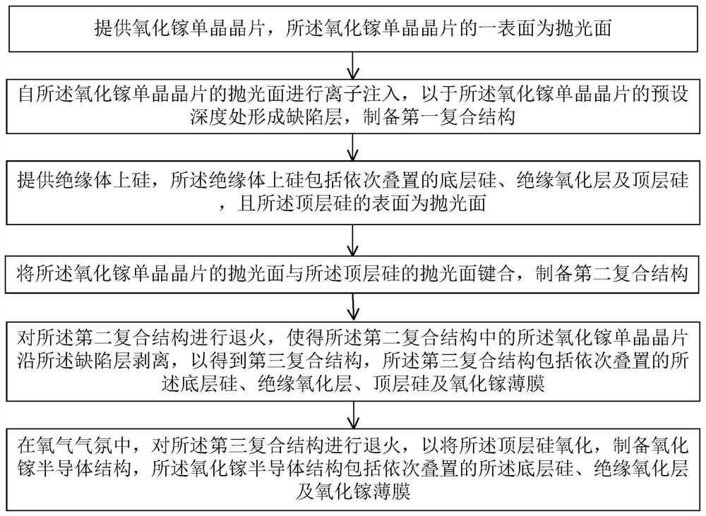
The invention provides a gallium oxide semiconductor structure, a solar-blind photodetector and a preparation method. The gallium oxide thin film can be successfully transferred by bonding the gallium oxide single crystal wafer to the top silicon in the silicon-on-insulator, and the bonding technology is mature. And by oxidizing the top layer of silicon in silicon-on-insulator, the problem of leakage can be effectively solved, high-quality, leakage-proof gallium oxide semiconductor structures can be prepared, and the performance of devices based on gallium oxide semiconductor structures can be improved. On the silicon substrate, the device is not only compatible with the CMOS process, but also can be mass-produced, which is of great significance for the rapid development of solar-blind photodetectors based on gallium oxide thin films.

Description

technical field [0001] The invention belongs to the field of semiconductor manufacturing, and relates to a gallium oxide semiconductor structure, a solar-blind photodetector and a preparation method. Background technique [0002] The third generation of wide bandgap semiconductors (bandgap E g >2.3eV) materials, including silicon carbide, zinc oxide, gallium nitride, gallium oxide, etc., due to the advantages of high breakdown voltage, high electron mobility, good thermal stability, and strong radiation resistance, more and more are applied to optoelectronic devices. [0003] Gallium oxide is a third-generation wide-bandgap semiconductor material with a band gap of 4.5eV to 4.9eV. It has the advantages of high light transmittance, good thermal stability, high mechanical strength, and simple preparation process. It is an ideal solar-blind ultraviolet sensitive material. At present, gallium oxide is difficult to achieve p-type doping, and it is still very difficult to he...

Claims


Application Information

Patent Timeline
Patent Type & Authority Patents(China)
IPC IPC(8): H01L31/18H01L31/0352H01L31/10
CPCH01L31/035272H01L31/10H01L31/186H01L31/1864H01L31/1896Y02E10/50Y02P70/50
Inventor 欧欣徐文慧游天桂沈正皓
Owner SHANGHAI INST OF MICROSYSTEM & INFORMATION TECH CHINESE ACAD OF SCI
Why Eureka
Try Eureka