Substrate-active layer composite nano photonics structure alkali metal compound photocathode

A technology of alkali metal compounds and nanophotons, which is applied in the manufacture of light-emitting cathodes, optics, optical components, etc., and can solve problems such as reducing light intensity

Pending Publication Date: 2020-07-31
EAST CHINA UNIV OF TECH
View PDF4 Cites 0 Cited by
  • Summary
  • Abstract
  • Description
  • Claims
  • Application Information

AI Technical Summary

Problems solved by technology

[0003] Although widely concerned, the performance of the alkali metal compound PEA photocathode still cannot meet the current application requirements, especially high-sensitivity low-light detection and high-brightness output, high QE and long-term operation that are urgently needed for advanced light sources that operate stably for a long time. Lifespan, improving QE can not only obtain high-current electron beams, but also reduce the light intensity required for a specific current intensity, thereby avoiding laser damage, reducing laser costs and reducing the adverse effects of photo-thermal conversion on lifespan
According to Spicer's three-step emission model, the valence band electrons of the PEA photocathode absorb photons and are excited to the conduction band high-energy state, and then diffuse and transport to the surface and escape from the material. The conduction band electrons must have an energy greater than the surface effective electron affinity. To achieve escape, that is, electrons need to be maintained in a high-energy state during the diffusion process, but the high-energy state electrons can easily return to the bottom of the conduction band through thermal relaxation, which leads to the effective transport distance of photoelectrons in the active region of the PEA cathode is much smaller than that of negative electrophiles. Negative Electron Affinity (NEA) cathode, so the effective thickness of the low active layer and high light reflectivity severely limit light absorption, which becomes the main factor affecting the QE of PEA cathode
However, there is no report on the application of the MSR effect of the nanophotonics structure in the photocathode of the alkali metal compound PEA.

Method used


Image

  • Substrate-active layer composite nano photonics structure alkali metal compound photocathode
  • Substrate-active layer composite nano photonics structure alkali metal compound photocathode
  • Substrate-active layer composite nano photonics structure alkali metal compound photocathode

Examples


Embodiment 1

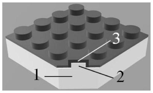
[0054] like figure 1 As shown, a substrate-active layer composite nano-cylindrical array photonics structure alkali metal compound photocathode, including substrate 1, nano-cylindrical array 2 and alkali metal compound active layer 3, the excitation light is active from the alkali metal compound The upper surface of the layer 3 is incident or incident from the lower surface of the substrate 1. When the light is incident from the lower surface of the substrate 1, the substrate 1 is made of a light-transmitting material. The process flow is as follows: firstly, the surface of the substrate 1 is Pretreatment, and then directly etching the upper surface of the substrate 1 to prepare the nano-cylindrical array 2, and finally depositing the alkali metal compound active layer 3 on the upper surface of the nano-cylindrical array 2; the specific preparation steps are as follows:

[0055] Step 1) Prepare the substrate 1

[0056] Prepare a circular SiO with a diameter of 3 inches and a ...

Embodiment 2

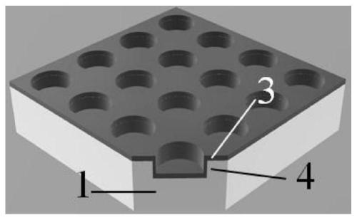
[0069] like figure 2 As shown, a substrate-active layer composite nano-cylindrical hole array photonics structure alkali metal compound photocathode, including a substrate 1, a nano-cylindrical hole array 4 and an alkali metal compound active layer 3, the laser is emitted from the alkali metal compound The upper surface of the source layer 3 is incident or incident from the lower surface of the substrate 1. When the light is incident from the lower surface of the substrate 1, the substrate 1 is made of a light-transmitting material. The process flow is as follows: firstly, the surface of the substrate 1 Perform pretreatment, then directly etch the upper surface of the substrate 1 to prepare the nano-cylindrical hole array 4, and finally deposit and prepare the alkali metal compound active layer 3 on the upper surface of the nano-cylindrical hole array 4; the specific preparation steps are as follows:

[0070] Step 1) Prepare the substrate 1

[0071] Prepare a circular SiO wi...


PUM

PropertyMeasurementUnit
Thicknessaaaaaaaaaa
Thicknessaaaaaaaaaa
Diameteraaaaaaaaaa

Abstract

The invention discloses a substrate-active layer composite nano photonics structure alkali metal compound photocathode. The photoelectric cathode sequentially comprises a substrate, a nano array and an alkali metal compound active layer from bottom to top, the optical resonance effect generated by the action of the nano array and incident light is utilized, the light reflectivity can be reduced, and the photoelectron generation and transportation efficiency is improved, so that the performance of the photoelectric cathode is effectively improved. According to the composite nano photonics structure alkali metal compound photocathode, the active layer is directly deposited and prepared on the upper surface of a nano array so as to avoid etching of a photoelectric emission surface; the nano array is prepared by directly etching the substrate by adopting mature processes such as nano imprinting or self-assembly nanospheres, the preparation process is simple, the stability is good, and thenano array can be applied to the fields of weak signal detection and imaging, biomedical treatment, accelerator electron sources, advanced light sources and the like.

Description

technical field [0001] The invention relates to the technical field of vacuum photoelectric emission and application, in particular to a substrate-active layer composite nanophotonic structure alkali metal compound photocathode. Background technique [0002] The working wavelength of the positron affinity (Positive Electron Affinity, PEA) alkali metal compound photocathode covers the ultraviolet to near-infrared light region, the quantum efficiency (Quantum efficiency, QE) is high, and the working life is long when the continuous output of strong beam current, The response speed can reach the picosecond level, and it has important application value in the technical fields of electron accelerators, advanced light sources, space detection technology, high-resolution night vision imaging, low-energy field emission electron microscopy, and electron beam lithography. Recently, with the development of science and technology, the requirements for the quality of the cathode are cons...

Claims


Application Information

Patent Timeline
IPC IPC(8): H01J9/12B81B7/04
CPCH01J9/12B81B7/04
Inventor 彭新村邹继军汤彬邓文娟朱志甫刘双飞
Owner EAST CHINA UNIV OF TECH
Why Eureka
Try Eureka