CO2 reflecting film based on silicon carbide substrate and preparation method thereof
A technology of silicon carbide and reflective film, applied in optics, instruments, optical components, etc., can solve technical difficulties and other problems, and achieve the effects of strong heat and humidity resistance, uniform linear expansion coefficient, and high elastic modulus
- Summary
- Abstract
- Description
- Claims
- Application Information
AI Technical Summary
Problems solved by technology
Method used
Image
Examples
Embodiment 1
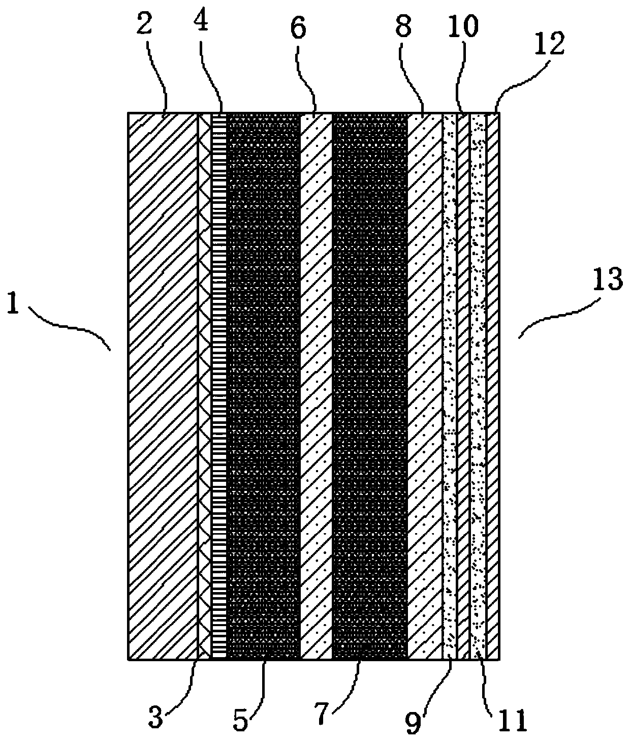
[0031] Such as image 3 As shown, the CO based on the SiC substrate 2 The reflective film includes a silicon carbide base layer, a diamond-like film layer, a nickel-chromium alloy adhesive layer, a metal film, a first germanium layer, a first zinc sulfide layer, a second germanium layer, a second zinc sulfide layer, The first YbF3 layer, the first ZnSe layer, the second YbF3 layer and the second ZnSe layer; the thickness of the diamond-like film layer is 1.2 μm, the thickness of the nickel-chromium alloy bonding layer is 0.2 μm, and the thickness of the metal film is 0.2 μm, The thickness of the first germanium layer is 1.7 μm, the thickness of the first zinc sulfide layer is 0.5 μm, the thickness of the second germanium layer is 1.7 μm, the thickness of the second zinc sulfide layer is 0.5 μm, and the thickness of the first YbF3 layer is 0.18 μm, the thickness of the first ZnSe layer is 0.08μm, the second YbF 3 The thickness of the layer is 0.18 μm and the thickness of the ...
Embodiment 2
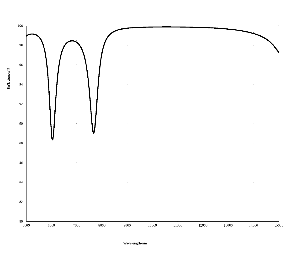
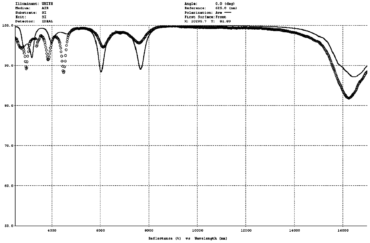
[0043] CO based on SiC substrates 2 Reflective film, the difference of embodiment 1 is: the thickness of the diamond-like film layer is 1.1 μm, the thickness of the nickel-chromium alloy bonding layer is 0.2 μm, the thickness of the metal film is 0.2 μm, and the thickness of the first germanium layer is 1.6 μm , the thickness of the first zinc sulfide layer is 0.6 μm, the thickness of the second germanium layer is 1.6 μm, the thickness of the second zinc sulfide layer is 0.6 μm, the thickness of the first YbF3 layer is 0.19 μm, and the thickness of the first ZnSe layer is 0.07μm, second YbF 3 The thickness of the layer is 0.19 μm and the thickness of the second ZnSe layer is 0.07 μm; the preparation method refers to Example 1; the infrared spectrophotometer Spectrum100 is used for index detection, and the single-sided reflection at 10600 nm reaches 99.8%, and the reflection at the red light reaches 80% ;
PUM
| Property | Measurement | Unit |
|---|---|---|
| thickness | aaaaa | aaaaa |
| thickness | aaaaa | aaaaa |
| thickness | aaaaa | aaaaa |
Abstract
Description
Claims
Application Information
 - R&D
- Intellectual Property
- Life Sciences
- Materials
- Tech Scout
- Unparalleled Data Quality
- Higher Quality Content
- 60% Fewer Hallucinations
Browse by: Latest US Patents, China's latest patents, Technical Efficacy Thesaurus, Application Domain, Technology Topic, Popular Technical Reports.
© 2025 PatSnap. All rights reserved.Legal|Privacy policy|Modern Slavery Act Transparency Statement|Sitemap|About US| Contact US: help@patsnap.com


