Manufacturing method of fan-out chip interconnection

A manufacturing method and fan-out technology, which is applied in semiconductor/solid-state device manufacturing, electrical components, electric solid-state devices, etc., can solve the problems of reducing the area of ​​functional parts, poor reliability, and large occupied area, so as to increase reliability, The effect of reducing the difficulty of interconnection and reducing the problem of open circuit and short circuit

Inactive Publication Date: 2020-08-07
ZHEJIANG UNIV
View PDF7 Cites 4 Cited by
  • Summary
  • Abstract
  • Description
  • Claims
  • Application Information

AI Technical Summary

Problems solved by technology

[0003] The traditional packaging technology installs various functional chips and passive devices on the substrate, which occupies a large area and has poor reliability, which cannot meet the trend of miniaturization of packaging systems. However, the three-dimensional heterogeneous packaging technology based on standard silicon technology (system-level Packaging SIP) uses TSV technology (Through Silicon Via, referred to as TSV, through-silicon via technology) and cavity structure to integrate chips with different substrates and different functions, which can realize chip stacking and interconnection in a small area, greatly Reducing the area of ​​functional parts and increasing their reliability is becoming more and more the direction of future development of the industry
[0004] However, due to the high complexity of the embedded chip process, the chip tends to be shifted inside the cavity. If there is a lot of shift, and the exposure of the subsequent wafer-level RDL (redistribution layer) process will also shift, Then there may be a short circuit or open circuit problem between the chip PAD (silicon chip pin) and the RDL line; also as the number of PADs in the subsequent chip increases, the gap between the PAD and the PAD becomes smaller and smaller, which is not conducive to Alignment for Embedded Wafer-Level Fan-Out Packaging

Method used


Image

  • Manufacturing method of fan-out chip interconnection
  • Manufacturing method of fan-out chip interconnection
  • Manufacturing method of fan-out chip interconnection

Examples


Embodiment 1

[0037] A method for fabricating fan-out chip interconnection, comprising:

[0038] A: Rewire the surface of the fan-out chip and introduce the PAD to the chip surface;

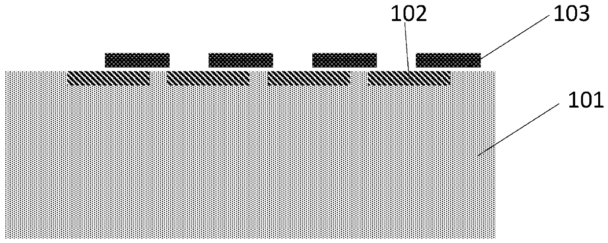
[0039] Such as figure 1 As shown, the chip 101 that needs to be embedded in the groove of the silicon interposer is coated with a photoresist or a passivation layer 103 on the surface. The photoresist can be positive or negative, with a thickness ranging from 1um to 100um. The oxide layer can be silicon oxide or silicon nitride with a thickness ranging from 10nm to 100um;

[0040] If it is photoresist, the PAD area 102 needs to be opened by an exposure process to expose the chip PAD;

[0041] If it is a passivation layer, the passivation layer in the PAD area needs to be removed by photolithography and etching;

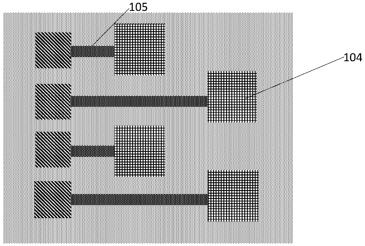
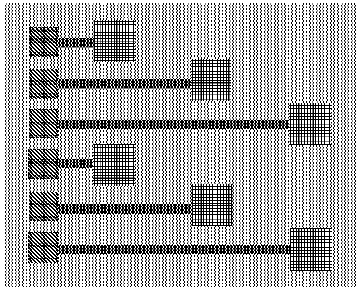
[0042] Then make the RDL interconnection circuit 105 on the chip surface, first make a seed layer on the insulating layer by physical sputtering, magnetron sputtering or evaporation process, the th...

Embodiment 2

[0050] A method for fabricating fan-out chip interconnection, comprising:

[0051]A: Cover the PAD on the surface of the fan-out chip with a passivation layer, and make a photoresist on the surface of the passivation layer;

[0052] Such as figure 1 As shown, the chip that needs to be embedded in the groove of the silicon interposer is coated with photoresist or passivation layer on the surface. The photoresist can be positive or negative, and the thickness ranges from 1um to 100um. The passivation layer It can be silicon oxide or silicon nitride with a thickness ranging from 10nm to 100um;

[0053] B: Perform photolithography and etching on the chip PAD to reduce the exposed interconnected metal area on the surface of the PAD;

[0054] If it is photoresist, it is necessary to use the exposure process to open the PAD area to expose the chip PAD;

[0055] If it is a passivation layer, the passivation layer in the PAD area needs to be removed by photolithography and etching; ...


PUM


Abstract

The invention discloses a fan-out chip interconnection manufacturing method, which comprises the steps: coating the surface of a fan-out chip with a photoresist or a passivation layer, and opening thephotoresist or the passivation layer covering the PAD region of the fan-out chip to expose the PAD of the fan-out chip; manufacturing an insulating layer on the surface of the fan-out chip, then manufacturing a seed layer above the insulating layer, then coating with an electroplating photoresist, electroplating with a metal to make RDL, then removing the photoresist, and then removing the seed layer; and connecting the other end of the RDL with the internal bonding pad, and remanufacturing an external bonding pad on the internal bonding pad. According to the invention, the size of the remanufactured external bonding pad is increased, and the distance between the bonding pads is increased; and the area and the position of the chip PAD are redefined, so that the difficulty of interconnection between the embedded fan-out chip PAD and the wafer-level RDL can be greatly reduced, the problems of open circuit and short circuit are reduced, and the reliability of the process is improved.

Description

technical field [0001] The invention relates to the field of semiconductors, in particular to a method for fabricating fan-out chip interconnections. Background technique [0002] Millimeter-wave radio frequency technology is developing rapidly in the semiconductor industry. It is widely used in high-speed data communications, automotive radar, airborne missile tracking systems, and spatial spectral detection and imaging. It is expected that the market will reach 1.1 billion US dollars in 2018 and become an emerging industry. New applications put forward new requirements for the electrical performance, compact structure and system reliability of the product. For the wireless transmitting and receiving system, it cannot be integrated into the same chip (SOC), so it is necessary to integrate different chips including radio frequency units. , filters, power amplifiers, etc. are integrated into an independent system to realize the functions of transmitting and receiving signals....

Claims


Application Information

Patent Timeline
Patent Type & Authority Applications(China)
IPC IPC(8): H01L21/60
CPCH01L24/02H01L2224/0231H01L2224/02379
Inventor 郁发新冯光建张兵王志宇
Owner ZHEJIANG UNIV
Why Eureka
Try Eureka