Diamond-based heterogeneously integrated gallium nitride thin film and transistor microelectronic device and preparation method thereof

A microelectronic device, gallium nitride single crystal technology, applied in the direction of semiconductor/solid-state device manufacturing, transistors, semiconductor devices, etc., to achieve the effect of long-term stable work

Inactive Publication Date: 2020-08-14
SHANGHAI INST OF MICROSYSTEM & INFORMATION TECH CHINESE ACAD OF SCI
View PDF11 Cites 12 Cited by
  • Summary
  • Abstract
  • Description
  • Claims
  • Application Information

AI Technical Summary

Problems solved by technology

[0005] The purpose of the present invention is to provide a diamond-based heterogeneously integrated gallium nitride thin film and transistor microelectronic device and its preparation method, so as to solve the problem in the prior art that it is impossible to directly integrate wafer-level single crystal GaN thin film and High-quality diamond substrate to solve GaN HEMT heat dissipation and improve performance

Method used


Image

  • Diamond-based heterogeneously integrated gallium nitride thin film and transistor microelectronic device and preparation method thereof
  • Diamond-based heterogeneously integrated gallium nitride thin film and transistor microelectronic device and preparation method thereof
  • Diamond-based heterogeneously integrated gallium nitride thin film and transistor microelectronic device and preparation method thereof

Examples


preparation example Construction

[0032] According to a preferred embodiment of the present invention, a method for preparing a diamond-based heterogeneously integrated gallium nitride thin film and transistor microelectronic device is provided, comprising the following steps:

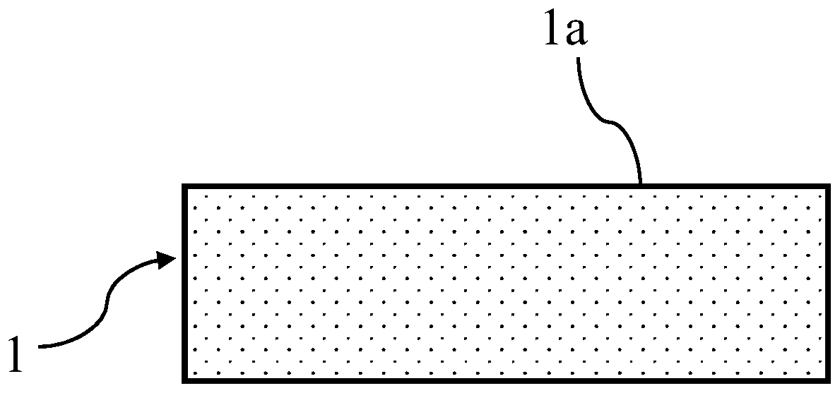
[0033] 1) Provide a gallium nitride single crystal wafer 1 with an injection surface 1a, such as figure 1 shown;

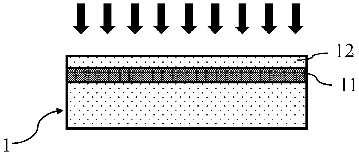
[0034] 2) From the injection surface 1a along figure 2 hydrogen ion implantation is carried out to the gallium nitride single crystal wafer 1 in the arrow direction of single crystal thin film 12, such as figure 2 shown;

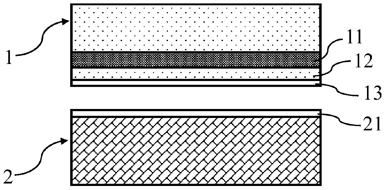
[0035] 3) growing a first dielectric layer 13 on the gallium nitride single crystal wafer 1, growing a layer of second dielectric layer 21 on the diamond support substrate 2, and using plasma to activate the surfaces of the first dielectric layer 13 and the second dielectric layer 21, Such as image 3 shown;

[0036] 4) bonding the first dielectric layer 13 with the second dielectric layer 21, su...

Embodiment 1

[0041] Provide millimeter-scale gallium nitride single crystal wafers. Perform hydrogen ion implantation from the implanted surface, the implantation energy is 75keV, and the implantation dose is 3.5×10 17 ions / cm 2 , an implanted defect layer is formed at a distance of about 500 nm from the implanted surface. A 5nm-thick nano-silicon dielectric layer is grown on a gallium nitride single crystal wafer and a 500μm-thick diamond support substrate and activated by argon plasma, and the nano-silicon dielectric layer is bonded in a vacuum environment, and the bonding temperature is is 20°C. Annealing treatment under vacuum, the annealing temperature is 550°C, and the annealing time is 2h. Chemical mechanical polishing removes the damaged layer. Next, the homoepitaxial growth is carried out on the surface of the GaN single crystal thin film by using the HEMT process to prepare the transistor.

[0042] combine Figure 7 The HEMT process steps are described in detail as follows,...

Embodiment 2

[0048] GaN monocrystalline wafers are provided at the wafer level. Perform hydrogen ion implantation from the implanted surface, the implantation energy is 35keV, and the implantation dose is 2.5×10 17 ions / cm 2 , an implanted defect layer is formed at a distance of about 300 nm from the implanted surface. The injection surface and the surface of the 200 μm thick diamond support substrate were directly bonded under a nitrogen atmosphere after being activated by nitrogen plasma, and the bonding temperature was 20°C. Annealing treatment under nitrogen atmosphere, the annealing temperature is 300°C, and the annealing time is 24h. The damaged layer was removed by ion beam etching, the energy was 2keV, the ambient temperature was 300°C, the incident angle of the ion beam was 60°, and the process time was 5min.

[0049] The HEMT process is the same as above, and a diamond-based heterogeneously integrated gallium nitride thin film and transistor microelectronic device is obtained....


PUM

PropertyMeasurementUnit
thicknessaaaaaaaaaa
thicknessaaaaaaaaaa
thicknessaaaaaaaaaa

Abstract

The invention provides a diamond-based heterogeneously integrated gallium nitride thin film and transistor microelectronic device and a preparation method thereof. The preparation method comprises thefollowing steps: S1, providing a gallium nitride single crystal wafer with an injection surface; S2, carrying out hydrogen ion implantation on the gallium nitride single crystal wafer from the injection surface so that implanted ions reach a preset depth, an injection defect layer is formed, and a gallium nitride single crystal thin film is formed above the injection defect layer; S3, bonding thegallium nitride single crystal thin film with a diamond support substrate; S4, performing annealing treatment to peel along the injection defect layer, and forming a damaged layer on the injection defect layer; S5, performing surface treatment to remove the damaged layer; and S6, performing homogeneous epitaxial growth on the surface of the gallium nitride single crystal thin film to prepare a transistor. The diamond-based gallium nitride transistor prepared according to the invention is greatly improved in performance, has the characteristics of high electron mobility and strong heat dissipation capability, can stably work for a long time in a high-frequency and high-power state, and has very remarkable superiority compared with the prior art.

Description

technical field [0001] The invention relates to the preparation of information functional materials and microelectronic devices, and more specifically relates to a diamond-based heterogeneously integrated gallium nitride thin film and transistor microelectronic device and a preparation method thereof. Background technique [0002] GaN is a wide bandgap semiconductor material with a direct bandgap of 3.4eV. GaN material has extremely strong stability and is insoluble in acid and alkali at room temperature. It is a hard high melting point material with a melting point of 1700°C and an elastic modulus of 398GPa. It is suitable for working in harsh environments (high temperature, high pressure, acid and alkali, etc.). An ideal material for microelectromechanical devices (MEMS). GaN has excellent optical properties and can be used to prepare devices such as blue light diodes (LEDs) and laser diodes (LDs). [0003] In addition, the breakdown electric field of GaN is extremely hi...

Claims


Application Information

Patent Timeline
Patent Type & Authority Applications(China)
IPC IPC(8): H01L21/335H01L29/778H01L29/10
CPCH01L29/7787H01L29/66462H01L29/1075H01L21/185
Inventor 欧欣石航宁伊艾伦游天桂张加祥黄凯王曦
Owner SHANGHAI INST OF MICROSYSTEM & INFORMATION TECH CHINESE ACAD OF SCI
Why Eureka
Try Eureka