Copper/ceramic bonded body, insulating circuit board, copper/ceramic bonded body production method, and insulating circuit board production method

A technology for circuit substrates and ceramic substrates, used in circuits, manufacturing tools, printed circuits, etc., can solve problems such as insufficient bonding, uneven melting conditions, and residues, and achieve the effect of suppressing excessive reaction.

Active Publication Date: 2020-08-21
MITSUBISHI MATERIALS CORP
View PDF17 Cites 0 Cited by
  • Summary
  • Abstract
  • Description
  • Claims
  • Application Information

AI Technical Summary

Problems solved by technology

[0011] However, as disclosed in Patent Document 1, when bonding a ceramic substrate and a copper plate by the DBC method, it is necessary to set the bonding temperature at 1065° C. or higher (above the eutectic point temperature of copper and copper oxide), so the ceramic substrate may deterioration
[0012] In addition, as disclosed in Patent Document 2, when a ceramic substrate and a copper plate are joined by an active metal brazing method, the brazing filler metal contains Ag, and Ag exists at the joint interface, so migration is likely to occur, so it cannot be used in high withstand voltage applications.
In addition, since the bonding temperature is relatively high at 900°C, there is still a problem of deterioration of the ceramic substrate.
[0013] In addition, as disclosed in Patent Document 3, the slurry contains powder composed of Cu-Mg-Ti alloy. When bonding under a nitrogen atmosphere using a solder for bonding composed of the slurry, there is residual gas at the bonding interface, which is likely to cause Partial Discharge Problem
Also, since the alloy powder is used, the melting state may become uneven depending on the composition deviation of the alloy powder, and a region with insufficient interfacial reaction may be locally formed.
In addition, organic matter contained in the slurry may remain at the bonding interface, resulting in insufficient bonding

Method used


Image

  • Copper/ceramic bonded body, insulating circuit board, copper/ceramic bonded body production method, and insulating circuit board production method
  • Copper/ceramic bonded body, insulating circuit board, copper/ceramic bonded body production method, and insulating circuit board production method
  • Copper/ceramic bonded body, insulating circuit board, copper/ceramic bonded body production method, and insulating circuit board production method

Examples


no. 1 approach

[0066] Below, refer to Figure 1 to Figure 4 , the first embodiment of the present invention will be described.

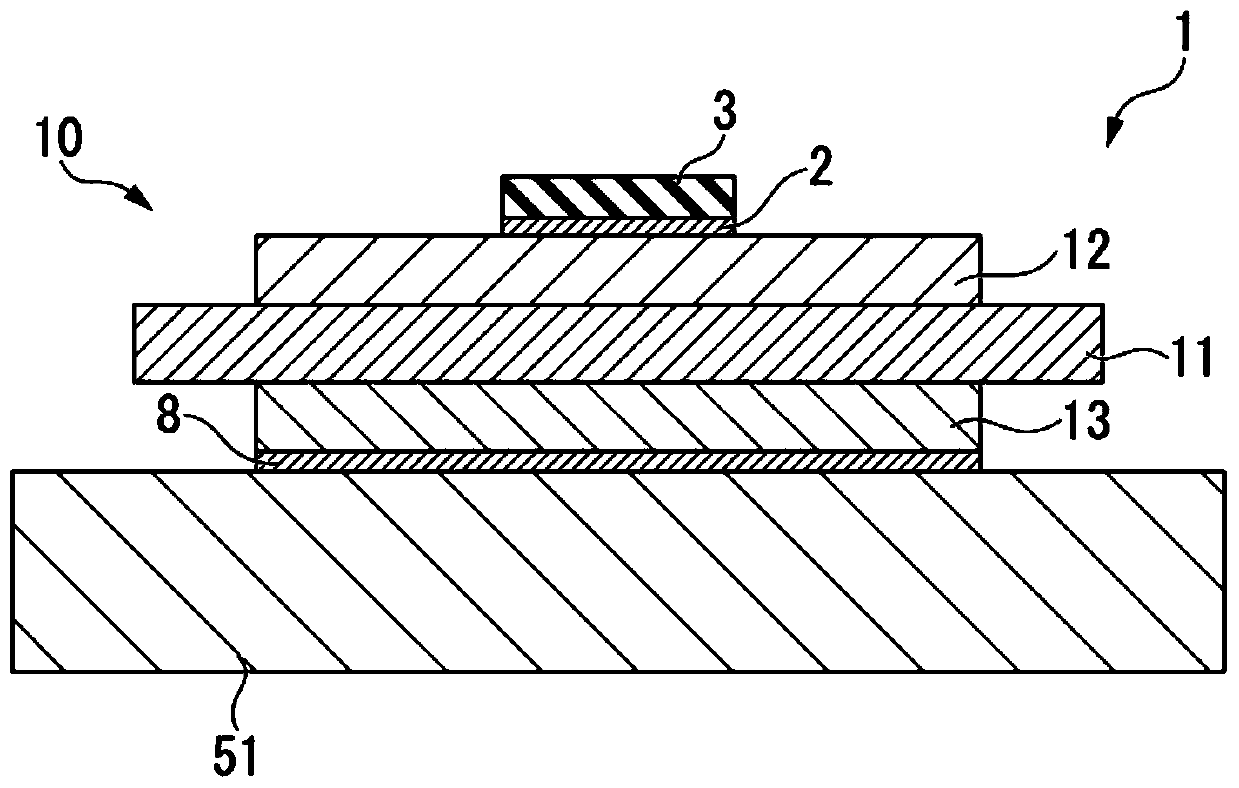
[0067] The copper-ceramic bonded body according to this embodiment is an insulated circuit board 10 constituted by bonding ceramic substrate 11 as a ceramic member and copper plate 22 (circuit layer 12 ) and copper plate 23 (metal layer 13 ) as copper members.

[0068] figure 1 In FIG. 2 , an insulating circuit board 10 according to the first embodiment of the present invention and a power module 1 using the insulating circuit board 10 are shown.

[0069] The power module 1 includes an insulating circuit substrate 10, and is bonded to one side of the insulating circuit substrate 10 via a first solder layer 2 ( figure 1 The semiconductor element 3 on the upper side) surface and the other side ( figure 1 The lower side of the middle) heat sink 51.

[0070] The insulating circuit substrate 10 includes a ceramic substrate 11, and is arranged on one surface of the c...

no. 2 approach

[0110] Next, refer to Figure 5 to Figure 8 , the second embodiment of the present invention will be described.

[0111] The copper-ceramic bonded body according to the present embodiment is an insulating circuit board 110 constituted by joining a ceramic substrate 111 as a ceramic member and a copper plate 122 (circuit layer 112 ) as a copper member.

[0112] Figure 5 2 shows an insulating circuit substrate 110 and a power module 101 using the insulating circuit substrate 110 as a second embodiment of the present invention.

[0113] The power module 101 includes an insulating circuit substrate 110, and is bonded to one side of the insulating circuit substrate 110 via a solder layer 2 ( Figure 5 The semiconductor element 3 on the upper side) and the other side of the insulating circuit substrate 110 ( Figure 5 The lower side of the middle) heat sink 151.

[0114] The solder layer 2 is made of, for example, a Sn-Ag-based, Sn-In-based or Sn-Ag-Cu-based solder material.

...

Embodiment

[0169] Confirmation experiments performed to confirm the effectiveness of the present invention will be described.

[0170]

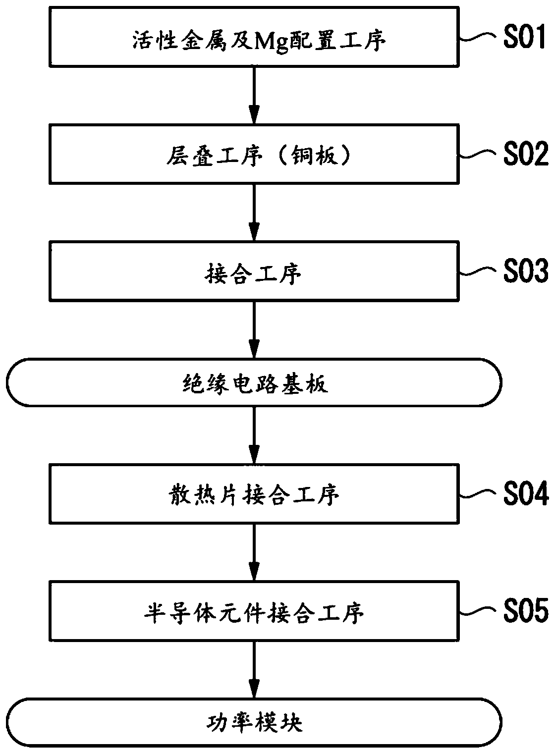
[0171] A copper-ceramic bonded body having the structure shown in Table 1 was formed. Specifically, as shown in Table 1, copper plates on which a simple substance of active metal and a simple substance of Mg were deposited were laminated on both sides of a 40 mm square ceramic substrate made of aluminum oxide, and joined under the joining conditions shown in Table 1. A copper-ceramic bonded body is formed. The thickness of the ceramic substrate was set to 0.635 mm. In addition, the vacuum degree of the vacuum furnace at the time of bonding was set to 5×10 -3 Pa.

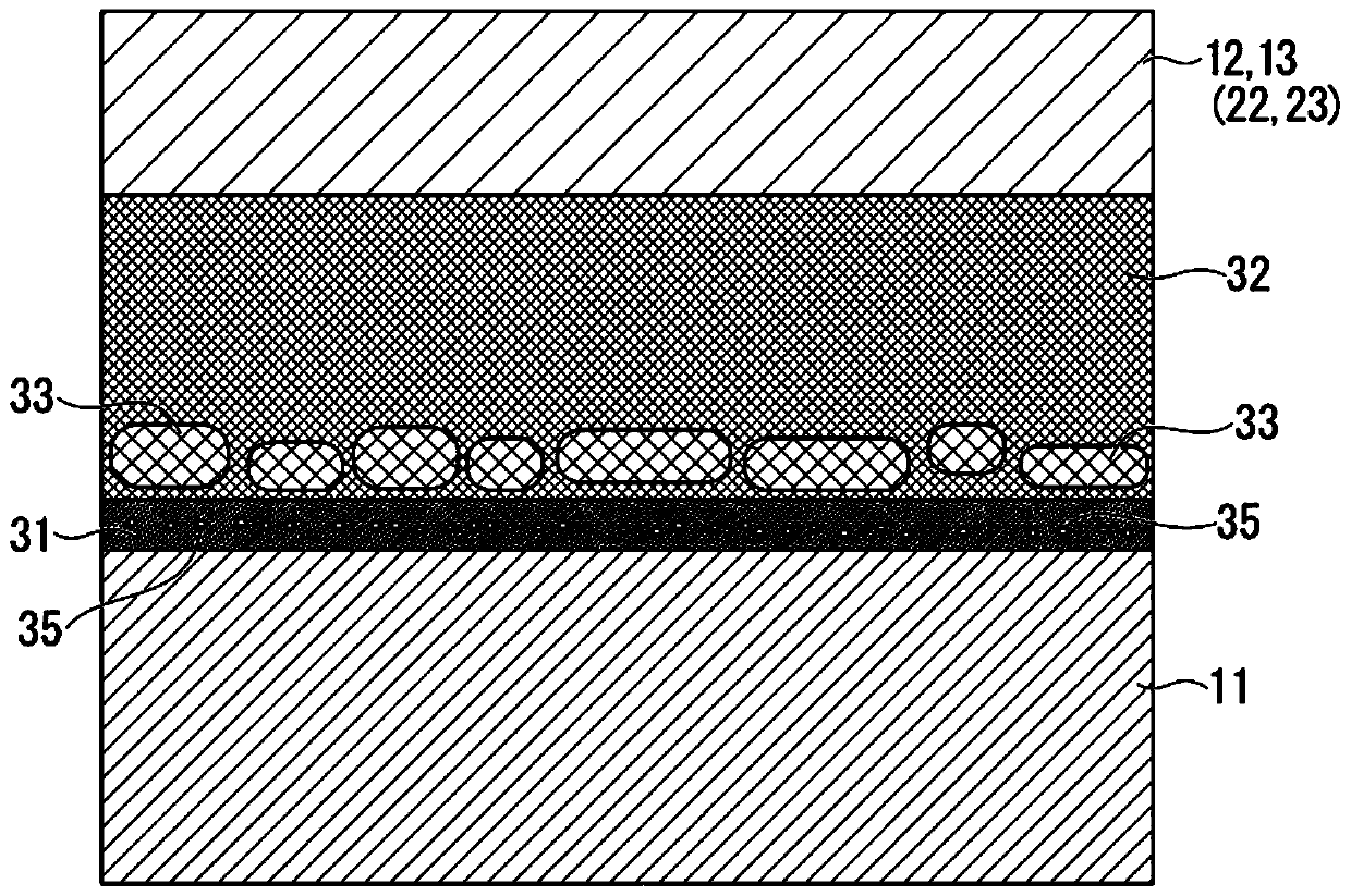
[0172] With regard to the copper-ceramic bonded body thus obtained, the presence or absence of Cu particles in the magnesium oxide layer, the Mg solid solution layer, the intermetallic compound phase, and the magnesium oxide layer, and the Cu concentration were confirmed by observing the bo...


PUM

PropertyMeasurementUnit
thicknessaaaaaaaaaa
thicknessaaaaaaaaaa
thicknessaaaaaaaaaa

Abstract

This copper/ceramic bonded body is constituted by a copper member (12), comprising copper or a copper alloy, and a ceramic member (11), comprising aluminum oxide, which are bonded to each other. A magnesium oxide layer (31) is formed between the copper member (12) and the ceramic member (11) on the ceramic member (11) side. A Mg solid solution layer (32) in which Mg is solid-solved in a Cu matrixphase is formed between the magnesium oxide layer (31) and the copper member (12). One or more active metals selected from Ti, Zr, Nb, and Hf are present in the Mg solid solution layer (32).

Description

technical field [0001] The present invention relates to a copper-ceramic bonded body formed by bonding a copper part made of copper or copper alloy and a ceramic part made of aluminum oxide, an insulating circuit substrate and a method for manufacturing the copper-ceramic bonded body, and an insulating circuit substrate Manufacturing method. [0002] This application claims priority based on Patent Application No. 2018-010965 filed in Japan on January 25, 2018 and Patent Application No. 2018-227472 filed in Japan on December 4, 2018, and the contents thereof are incorporated herein. Background technique [0003] In a power module, an LED module, and a thermoelectric module, a power semiconductor element, an LED element, and a thermoelectric element are bonded to an insulating circuit substrate in which a circuit layer made of a conductive material is formed on one side of an insulating layer. [0004] Power semiconductor elements for high-power control, such as wind power g...

Claims


Application Information

Patent Timeline
Patent Type & Authority Applications(China)
IPC IPC(8): C04B37/02H01L23/12H01L23/13H01L23/36
CPCH01L23/13H01L23/12H01L23/36C04B37/02B23K1/0016B23K1/008B23K1/19B23K1/20B23K20/026B23K20/16B23K20/233B23K20/24B23K2101/42B23K2103/12B23K2103/18B23K2103/52C04B35/645C04B37/023C04B37/026C04B2235/6567C04B2235/6581C04B2237/06C04B2237/064C04B2237/09C04B2237/12C04B2237/121C04B2237/122C04B2237/124C04B2237/126C04B2237/127C04B2237/128C04B2237/343C04B2237/407C04B2237/55C04B2237/592C04B2237/60C04B2237/704C04B2237/708C04B2237/72H01L23/3735H01L2224/32225C04B2237/525B23K20/165H01L23/142H01L23/3731
Inventor 寺崎伸幸
Owner MITSUBISHI MATERIALS CORP
Why Eureka
Try Eureka