Ceramic substrate porous array picosecond laser galvanometer scanning drilling system and method

A technology of ceramic substrates and porous arrays, applied in laser welding equipment, welding equipment, metal processing equipment, etc., can solve the problems of reduced processing efficiency, low cutting efficiency, and increased procedures, so as to improve processing efficiency, position accuracy, and yield The effect of improving and increasing the cutting speed

Inactive Publication Date: 2020-08-28
苏州优快激光科技有限公司
View PDF24 Cites 15 Cited by
  • Summary
  • Abstract
  • Description
  • Claims
  • Application Information

AI Technical Summary

Problems solved by technology

[0003] Patent document CN110605488A discloses a ceramic laser drilling device. The invention uses a three-axis laser drilling system with xy+ cyclotron vibration for ceramic drilling of electronic and semiconductor devices, but it does not refer to what kind of laser is used. , and did not describe the drilling process in detail. In addition, cutting a circle with a larger diameter through a circular motion will result in low cutting efficiency due to the inertia of the machine itself.
[0004] Patent document CN105499812A discloses a method for improving the processing quality of ceramic heat dissipation substrates. The invention relates to a laser processing method for LED ceramic heat dissipation substrates. To solve the problems of oxidation and yellowing of the ceramic substrate during the drilling process, although the processing quality has been improved, the process has been significantly increased and the processing efficiency has been reduced. In addition, the laser used is also a conventional continuous solid-state laser.

Method used


Image

  • Ceramic substrate porous array picosecond laser galvanometer scanning drilling system and method
  • Ceramic substrate porous array picosecond laser galvanometer scanning drilling system and method
  • Ceramic substrate porous array picosecond laser galvanometer scanning drilling system and method

Examples


Embodiment Construction

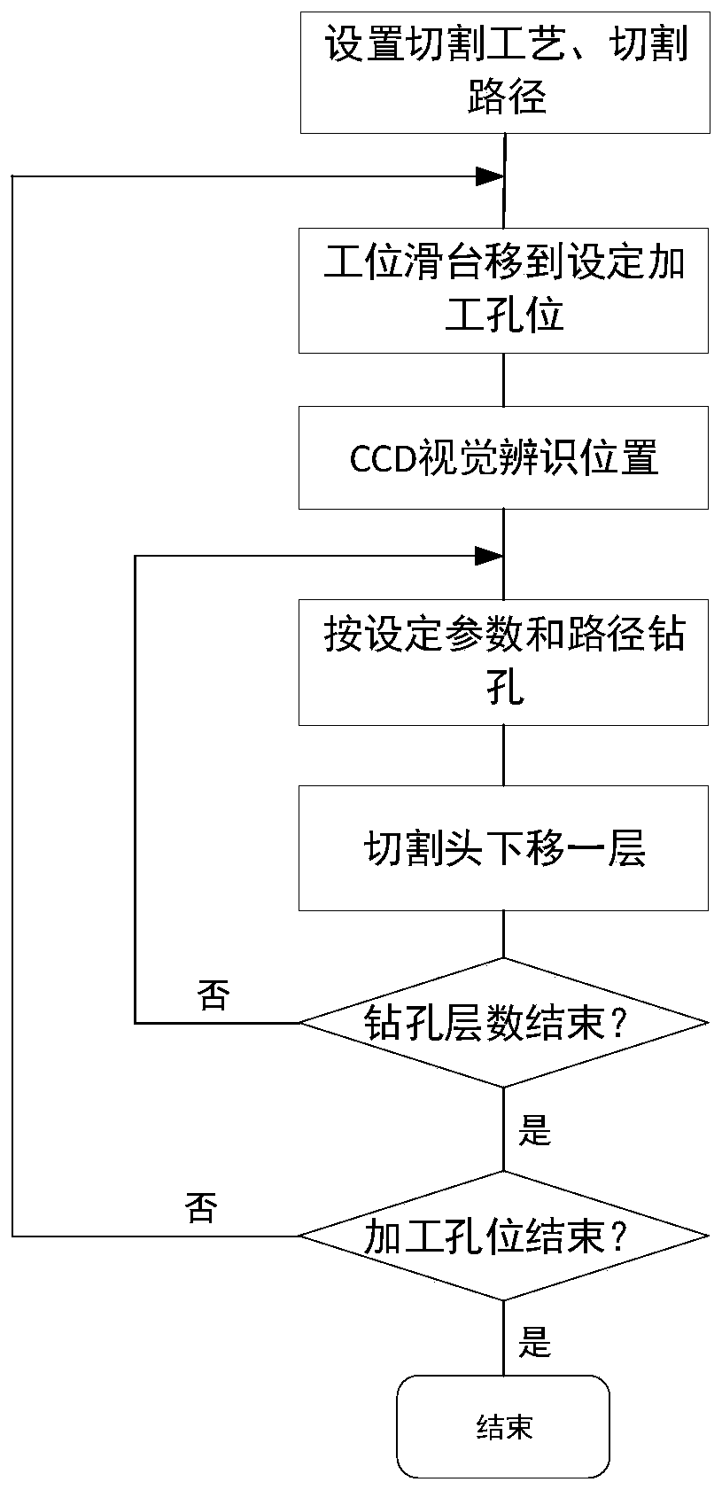
[0032] The present invention will be described in detail below in conjunction with specific embodiments. The following examples will help those skilled in the art to further understand the present invention, but do not limit the present invention in any form. It should be noted that those skilled in the art can make several changes and improvements without departing from the concept of the present invention. These all belong to the protection scope of the present invention.

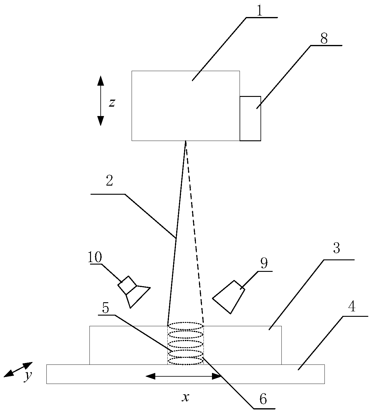
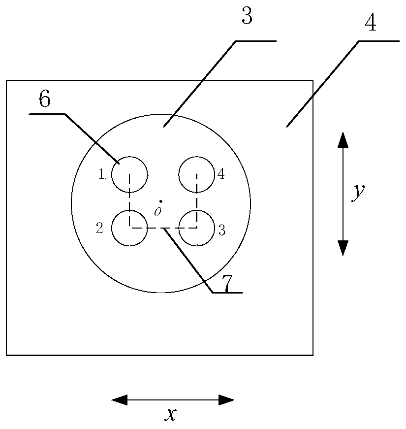
[0033] According to the present invention, a porous array picosecond laser vibrating mirror scanning drilling system for ceramic substrates includes: scanning vibrating mirror 1, scanning laser beam unit 2, substrate 3, xy two-dimensional slide table 4, layered processing path 5, Processing hole position 6, porous array processing path 7, visual components 8, protective gas nozzle 9, smoke suction cover 10; the scanning vibrating mirror 1 is arranged on the upper part of the ceramic substrate porous arra...


PUM

PropertyMeasurementUnit
diameteraaaaaaaaaa

Abstract

The invention provides a ceramic substrate porous array picosecond laser galvanometer scanning drilling system and method. The method comprises the steps that firstly a laser drilling route and a laser drilling technological parameter are arranged, during drilling, a station sliding table moves a hole to be drilled of a ceramic substrate to a drilling position, CCD vision identifies and positionsthe drilling position, and a galvanometer laser beam precisely drills the ceramic substrate layer by layer; meanwhile, smoke suction and protective gas are started, a cutting head automatically movesdown one layer of machining thickness for each layer machining until all the layers are machined; and then the station sliding table moves a workpiece to the next drilling position, repetition is carried out until all the holes in the ceramic substrate are drilled. According to the ceramic substrate porous array picosecond laser galvanometer scanning drilling system and method, cutting edges of the ceramic substrate are smooth, the roundness is good, the taper is small, the fragmentation probability is low, nearly no heat affected zone exists, the edges are not yellowed, nearly no damage is caused to the ceramic substrate, and the yield is greatly improved.

Description

technical field [0001] The invention relates to the field of laser processing, in particular to a porous array picosecond laser vibrating mirror scanning drilling system and method for a ceramic substrate. Background technique [0002] Ceramic materials such as alumina and aluminum nitride have the advantages of high thermal conductivity, high insulation and high temperature resistance, and are widely used in the fields of electronics and semiconductors. However, ceramic materials have high hardness and brittleness, and their forming and processing are very difficult, especially the processing of micropores. Due to the high power density and good directionality of the laser, lasers are commonly used to drill holes in ceramic substrates. At present, pulsed lasers or quasi-continuous lasers are generally used. The laser beam is focused on a laser beam placed perpendicular to the laser axis through an optical system. On the workpiece, a laser beam with high energy density (105...

Claims


Application Information

Patent Timeline
Patent Type & Authority Applications(China)
IPC IPC(8): B23K26/03B23K26/08B23K26/12B23K26/16B23K26/382B23K26/402B23K26/70
CPCB23K26/382B23K26/402B23K26/0853B23K26/032B23K26/16B23K26/12B23K26/702
Inventor 张轲龚朋真
Owner 苏州优快激光科技有限公司
Why Eureka
Try Eureka