Preparation method and application of copper-copper bonding material

A bonding material, copper-copper bonding technology, used in semiconductor/solid-state device manufacturing, electrical components, circuits, etc. Thermodynamic properties, the effect of reducing production equipment requirements, and reducing production costs

Inactive Publication Date: 2020-09-01
苏州清飙科技有限公司
View PDF7 Cites 3 Cited by
  • Summary
  • Abstract
  • Description
  • Claims
  • Application Information

AI Technical Summary

Problems solved by technology

[0006] 2) In a short period of time at low temperature, the copper on both sides of the interface diffuses to achieve the bonding strength, which requires strong diffusion characteristics under low temperature conditions. However, for ordinary metal copper, the diffusion coefficient usually does not meet this requirement;
[0007] 3) The consistency of the height of the electroplated copper pillars is relatively poor, resulting in the fact that the copper pillars on both sides and the copper pillars or the copper pillars and the pads may not be in the same plane during copper-copper bonding, and copper has a relatively high Young's modulus so that It is necessary to consider that when the wafer warpage and the height of the copper pillars are not completely consistent, there will be local inaccessibility or stress concentration caused by forced bonding during the stacking process.
However, there is a problem with this method. Due to the local difference in the design distribution density of the copper pillar pattern, the current density in the dense area will be low, and the current density in the sparse area will be high. It is difficult to guarantee that all copper pillars that need to be bonded can be coplanar
In addition, most electroplated nano-twinned copper has a relatively large surface roughness. Based on such a surface, it is relatively difficult to obtain a high bonding force through diffusion. However, if chemical mechanical polishing is used, the process will be increased, and the cost will be reduced. production efficiency, lower yield

Method used


Image

  • Preparation method and application of copper-copper bonding material
  • Preparation method and application of copper-copper bonding material

Examples


preparation example Construction

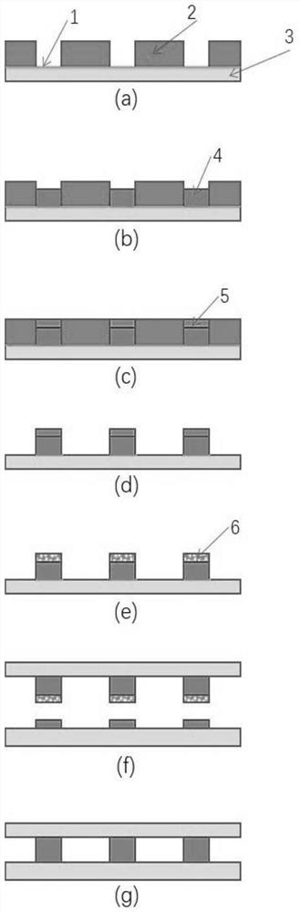
[0042] The preparation method of the copper-copper bonding material according to the embodiment of the present invention comprises the following steps:

[0043]Step S1, setting a nanoporous copper foam layer on the surface to be welded of at least one object to be welded;

[0044] In step S2, the surfaces to be welded of the object to be welded are arranged opposite to each other, and thermocompression bonding is performed to realize copper-copper bonding between the objects on both sides to be welded, and the copper-copper bonding material is obtained.

[0045] That is to say, according to the preparation method of the copper-copper bonding material of the embodiment of the present invention, a nanoporous copper foam layer is first arranged on at least one surface to be welded, and then the nanoporous copper foam layer is opposite to the surface to be welded on the other side. , to achieve copper-copper bonding by thermocompression bonding.

[0046] According to the preparat...

Embodiment 1

[0080] According to 0.0025mol / L copper sulfate CuSO 4 ·5H 2 O, 0.15mol / L zinc sulfate ZnSO 4 , 0.35mol / L potassium pyrophosphate K 4 P 2 o 7 , each reagent was weighed and added into pure water, stirred thoroughly and then dissolved, after which the pH value was adjusted to 7 by concentrated sulfuric acid to obtain an electroplating solution.

[0081] Thereafter, as the sample to be plated will be as figure 1 The silicon wafer shown in (a) that has completed the exposure and development process is placed in the electroplating solution, and a platinum anode is placed in the electroplating solution, and 0.2ASD is used for electroplating for 180 minutes to obtain a copper-zinc alloy layer. After that, take out the electroplated silicon wafer, remove the photoresist layer, wash the surface with pure water, dry it with cold air, and bake it at 200°C for 15 minutes under the protection of nitrogen to reform the copper-zinc alloy coating.

[0082] Then, the silicon wafer is put...

Embodiment 2

[0089] According to 0.0045mol / L copper sulfate CuSO 4 ·5H 2 O, 0.3mol / L zinc sulfate ZnSO 4 , 0.5mol / L potassium pyrophosphate K 4 P 2 o 7 , each reagent was weighed and added into pure water, stirred thoroughly and then dissolved, after which the pH value was adjusted to 8 by concentrated sulfuric acid to obtain an electroplating solution.

[0090] Thereafter, the same silicon wafer as in Example 1 was placed in the electroplating solution, and a platinum anode was placed in the electroplating solution, and 0.5ASD was used for electroplating for 90 minutes to obtain a copper-zinc alloy layer. After that, take out the electroplated silicon wafer, remove the photoresist layer, wash the surface with pure water, dry it with cold air, and bake it at 180°C for 30 minutes under the protection of nitrogen to reform the crystal grains in the copper-zinc alloy coating.

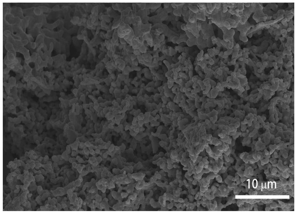
[0091] Then, the wafer is placed in a dealloying solution to remove the zinc from the alloy. The dealloying so...


PUM

PropertyMeasurementUnit
Elastic modulusaaaaaaaaaa
Thicknessaaaaaaaaaa
Thicknessaaaaaaaaaa

Abstract

The invention provides a preparation method and application of a copper-copper bonding material. The preparation method of the copper-copper bonding material comprises the following steps that S1, a nano-porous copper foam layer is arranged on to-be-welded surfaces of at least one to-be-welded object; and S2, the to-be-welded faces of the to-be-welded object are oppositely arranged, hot-pressing bonding is carried out, copper-copper bonding is achieved between the to-be-welded objects on the two sides, and the copper-copper bonding material is obtained. According to the preparation method of the copper-copper bonding material, high-density all-copper interconnection is obtained, copper-copper bonding does not contain any organic matter, good electrical and thermodynamic properties are achieved, the problem that holes are generated due to volatilization of the organic matter is avoided even if the copper-copper bonding material is used at a relatively high temperature, and due to the fact that copper is arranged on the two sides of a bonding interface, and Kirkendall holes of a copper-tin interface caused by copper-tin diffusion coefficient difference are avoided.

Description

technical field [0001] The invention relates to the technical field of electronic material preparation, in particular to a preparation method and application of a copper-copper bonding material. Background technique [0002] The increasing I / O density requirements of the electronics industry are driving demand for chips. At present, the pitch of the packaging substrate (C2S, Chip to Substrate) has been reduced to less than 20 μm, and the diameter of the copper pillar is also close to 10 μm, which is close to the limit of the copper pillar solder cap technology. Such extreme scaling requires further reduction in solder volume, increased solder cap bridging strength, and improved reliability. [0003] In addition, the traditional solder is pure tin or tin silver, which is used to solder copper pillars. Due to the difference in the diffusion coefficient of copper and tin, Kirkendall holes will appear at the copper-tin interface. In contrast, copper-copper bonding is also comp...

Claims


Application Information

Patent Timeline
IPC IPC(8): C25D3/56C25D5/50C25D7/12C23F1/44C23F1/30C23G1/10H01L21/603
CPCC25D3/565C25D5/50C25D7/12C23F1/44C23F1/30C23G1/103H01L24/83H01L2224/83024H01L2224/83203H01L2224/81895
Inventor 胡斌
Owner 苏州清飙科技有限公司
Why Eureka
Try Eureka