Method for realizing hole local passivation contact, and crystalline silicon solar cell and preparation method thereof

A crystalline silicon, local technology, applied in the field of solar cell preparation, can solve the problems of difficult application of local passivation contact structure, cumbersome preparation steps, cumbersome process steps, etc., and achieves less photogenerated carrier transmission loss, simple process, high photogenerated Effect of carrier collection probability

Inactive Publication Date: 2020-09-04
CHANGZHOU SHICHUANG ENERGY CO LTD
View PDF7 Cites 17 Cited by
  • Summary
  • Abstract
  • Description
  • Claims
  • Application Information

AI Technical Summary

Problems solved by technology

Photolithography belongs to the manufacturing method of semiconductor chips, the cost is high and the preparation steps are cumbersome; and the use of chemical slurry etching to prepare local contact passivation structures also requires doping on the polysilicon layer, preparing masks, printing protective or Etching-type chemical slurry, chemical etching, and mask removal, etc., the preparation steps are cumbe

Method used


Image

  • Method for realizing hole local passivation contact, and crystalline silicon solar cell and preparation method thereof
  • Method for realizing hole local passivation contact, and crystalline silicon solar cell and preparation method thereof
  • Method for realizing hole local passivation contact, and crystalline silicon solar cell and preparation method thereof

Examples


Embodiment 3

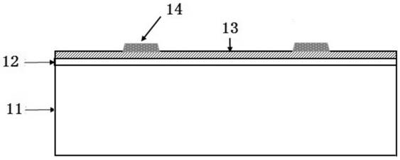
[0072] Embodiment 3 discloses a solar cell structure with a hole local passivation contact structure and a preparation method thereof. The battery structure given in this embodiment is as follows image 3 As shown, the front side of the battery adopts hole-local passivation contacts, and the back side of the battery adopts full-area electron passivation contacts. The substrate material here is n-type single crystal silicon (or p-type single crystal silicon).

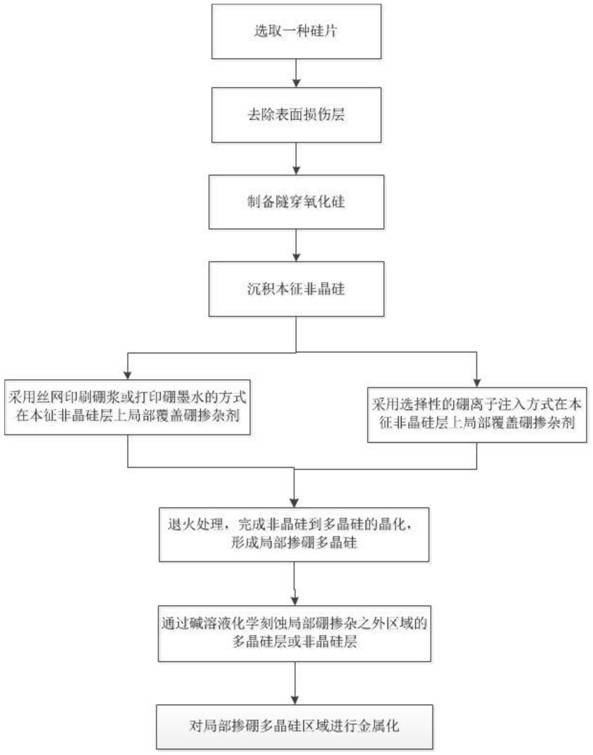
[0073] The preparation method of the battery is as follows:

[0074] A1: Select a 156mm*156mm (100) n-type monocrystalline silicon wafer with a resistivity of 1 Ω·cm and a thickness of 180 μm.

[0075] A2: NaOH polishing is used to remove the damaged layer (about 10 μm) on the surface of the n-type silicon wafer.

[0076]A3: A tunneling silicon oxide layer is prepared on both sides of the n-type silicon wafer by a thermal oxidation process, with a thickness of 1.5 nm and a refractive index of 1.46.

[0077] A4: Intri...

Embodiment 4

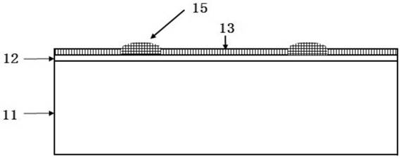
[0087] Embodiment 4 discloses another solar cell structure with a hole-local passivation contact structure and its preparation method. The battery structure given in this embodiment is as follows Figure 4 As shown, the front side of the battery adopts hole local passivation contact, and the back side of the battery adopts n-type doped junction and corresponding passivation film. In this example, the substrate material is p-type single crystal silicon. The battery preparation method is as follows:

[0088] B1: Choose a p-type monocrystalline silicon wafer with a (100) crystal orientation of 156mm*156mm, a resistivity of 1 Ω·cm, and a thickness of 180 μm.

[0089] B2: Polishing with sodium hydroxide solution to remove the damaged layer (about 10 μm) on the surface of the p-type silicon wafer.

[0090] B3: A tunneling silicon oxide layer is prepared on the surface of the p-type silicon wafer by a thermal oxidation process, with a thickness of 1.3 nm and a refractive index of ...


PUM

PropertyMeasurementUnit
Thicknessaaaaaaaaaa
Thicknessaaaaaaaaaa
Resistivityaaaaaaaaaa

Abstract

The invention discloses a method for realizing hole local passivation contact, which can realize selective boron doping by adopting printing boron slurry or printing boron ink, and can also realize selective boron doping by selective boron ion implantation, and the boron surface concentration of the formed local boron-doped polycrystalline silicon is not lower than 7E19cm <-3>; and the polycrystalline silicon or amorphous silicon thin film region without local boron doping is etched through alkaline solution chemical etching, and the local boron-doped polycrystalline silicon region is metalized to form the hole local passivation contact structure. Furthermore, the invention also discloses a crystalline silicon solar cell with the hole local passivation contact structure and a correspondingcell preparation method. According to the preparation method of the hole local passivation contact and the preparation method of the corresponding crystalline silicon solar cell, the process is simple, the cost is low, and the industrial potential is good.

Description

technical field [0001] The invention belongs to the technical field of solar cell preparation, and in particular relates to a method for realizing a partial hole passivation contact structure, and applying the hole partial passivation contact structure to a crystalline silicon solar cell and a corresponding cell preparation method. Background technique [0002] Passivated contact (Tunnel Oxide and Passivated Contact, TOPCon) solar cell is a new type of high-efficiency solar cell, which passivates crystalline silicon solar cells (hereinafter referred to as solar cells or cells) by tunneling silicon oxide and doped polycrystalline silicon. surface, to realize the selective passage of photogenerated carriers, that is, the majority carriers can enter the doped polysilicon film through the tunneling silicon oxide layer without hindrance and then be collected, while the minority carriers are in the tunnel The recombination rate at the interface of the silicon oxide and silicon is ...

Claims


Application Information

Patent Timeline
IPC IPC(8): H01L31/18H01L31/0224H01L31/0216H01L31/068
CPCH01L31/02168H01L31/022425H01L31/068H01L31/1804H01L31/1864H01L31/1868Y02E10/546Y02E10/547Y02P70/50
Inventor 黄海冰张梦葛沈梦超张胜军绪欣吴智涵
Owner CHANGZHOU SHICHUANG ENERGY CO LTD
Why Eureka
Try Eureka