Gate drive circuit and drive method of silicon carbide device

A gate drive, silicon carbide technology, applied in the field of circuits, can solve the problems of current overshoot, increase device loss, affect system efficiency, electromagnetic compatibility and other performance problems

Pending Publication Date: 2020-09-11
长沙丹芬瑞电气技术有限公司
View PDF7 Cites 0 Cited by
  • Summary
  • Abstract
  • Description
  • Claims
  • Application Information

AI Technical Summary

Problems solved by technology

[0003] Although SiC MOSFET has many advantages in application, because of its very high switching speed, SiC MOSFET is very sensitive to the packaging, wiring, stray parasitic inductance of the line and the device's own node capacitance, mainly reflected in Under the application of high voltage, high power and high switching speed, it is easy to generate high voltage change rate (dv/dt) and current change rate (di/dt) when SiC MOSFET is turned on and off, resulting in current overshoot and voltage overshoot. Problems such as shock and long-term switching oscillation will significantly increase device loss, seriously affect system efficiency, electromagnetic compatibility and other performance, and reduce system reliability
[0004] In order to protect SiC devices, measures are usually taken to suppress overcurrent and overvoltage. Although the existing method of variable drive resistance can delay the rise and fall time of the current, it increases the switching delay and Miller plateau time, making the SiC MOSFET generate larger The switching loss affects the efficiency of the converter; although the existing method of adding a snubber circuit can effectively reduce the turn-off overvoltage of the SiC MOSFET, it

Method used


Image

  • Gate drive circuit and drive method of silicon carbide device
  • Gate drive circuit and drive method of silicon carbide device
  • Gate drive circuit and drive method of silicon carbide device

Examples


Embodiment Construction

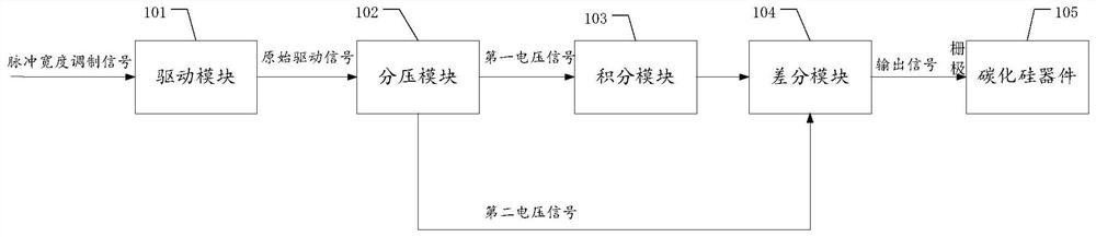
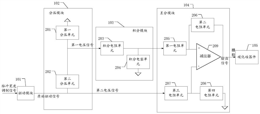
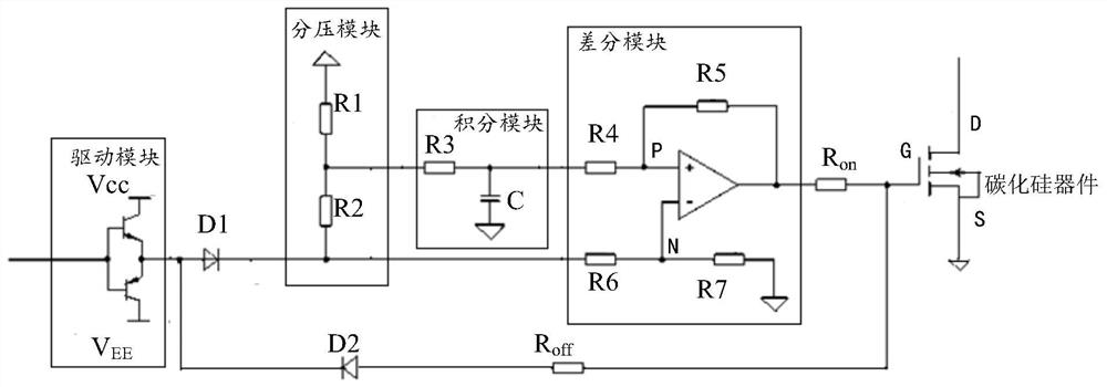
[0061] The core of the present invention is to provide a gate drive circuit and a driving method of a silicon carbide device, which can suppress the current overshoot in the conduction process, effectively improve the reliability of the circuit system, and reduce the conduction loss of the silicon carbide device.

[0062] In order to make the purpose, technical solutions and advantages of the embodiments of the present invention clearer, the technical solutions in the embodiments of the present invention will be clearly and completely described below in conjunction with the drawings in the embodiments of the present invention. Obviously, the described embodiments It is a part of embodiments of the present invention, but not all embodiments. Based on the embodiments of the present invention, all other embodiments obtained by persons of ordinary skill in the art without making creative efforts belong to the protection scope of the present invention.

[0063] Generally, the condu...


PUM


Abstract

The invention discloses a gate drive circuit and a gate drive method of a silicon carbide device, which can suppress current overshoot in a conduction process, effectively improve the reliability of acircuit system and reduce the conduction loss of the silicon carbide device. The gate drive circuit comprises a drive module, a voltage division module, an integration module and a differential module. The driving module generates an original driving signal according to the pulse width modulation signal; the voltage division module performs voltage division processing on the original driving signal to obtain a first voltage signal and a second voltage signal, sends the first voltage signal to the integration module, and sends the second voltage signal to the differential module; the integration module performs delay processing of preset time on the first voltage signal; and the difference module performs difference operation on the first voltage signal and the second voltage signal afterdelay processing to obtain an output signal, so that the output signal is the second voltage signal before the preset time, and the voltage value of the output signal is smaller than the voltage valueof the second voltage signal after the preset time.

Description

technical field [0001] The invention relates to the field of circuits, in particular to a gate drive circuit and a drive method of a silicon carbide device. Background technique [0002] Traditional silicon (Si) material power devices have a narrow bandgap and low blocking voltage. It is difficult to meet the requirements of the new generation of power systems in terms of energy consumption, operating temperature and switching frequency, which has become a bottleneck in the development of power electronics technology. Silicon carbide (SiC) is a new type of semiconductor material with wide bandgap and high breakdown voltage. Its bandgap width is about 3 times that of Si material, and its breakdown voltage is more than 10 times that of Si material. Compared with traditional Si-based power devices, SiC MOSFET has the advantages of higher blocking voltage, lower on-state resistance, good thermal conductivity, high-speed breaking capability, etc. It is used in electric vehicle dr...

Claims


Application Information

Patent Timeline
IPC IPC(8): H03K17/042H03K17/082
CPCH03K17/04206H03K17/0822
Inventor 张勇刘平
Owner 长沙丹芬瑞电气技术有限公司
Why Eureka
Try Eureka