Preparation method of super-hydrophobic surface with multi-scale structure

A super-hydrophobic, multi-scale technology, applied in the photolithographic process of the patterned surface, the process for producing decorative surface effects, microstructure technology, etc., can solve the problems of easy damage, loss of surface super-hydrophobicity, etc. Achieve the effect of prolonging service life, reducing processing cost and reducing difficulty

Active Publication Date: 2020-09-25
XI AN JIAOTONG UNIV
View PDF9 Cites 4 Cited by
  • Summary
  • Abstract
  • Description
  • Claims
  • Application Information

AI Technical Summary

Problems solved by technology

However, in a complex water environment, the C-B state is easily destroyed, los

Method used


Image

  • Preparation method of super-hydrophobic surface with multi-scale structure
  • Preparation method of super-hydrophobic surface with multi-scale structure
  • Preparation method of super-hydrophobic surface with multi-scale structure

Examples


preparation example Construction

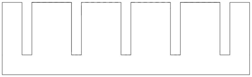
[0031] see Figure 1 to Figure 5 , a method for preparing a multi-scale structure super-hydrophobic performance surface, comprising the following steps:

[0032] Step 1, spin-coating a layer of positive photoresist on the silicon substrate, and exposing with a mask plate with a light-transmitting grid array;

[0033] Step 2, putting the structure obtained after exposure in step 1 into a developing solution for development to obtain a silicon wafer substrate with a grid-shaped raised photoresist array;

[0034] Step 3, processing the silicon wafer substrate obtained in step 2 in an oxygen plasma dry degumming machine to obtain a degummed and clean silicon wafer substrate;

[0035] Step 4, processing the silicon substrate obtained in step 3 by wet etching to obtain a silicon substrate with a grid-type protrusion array;

[0036] Step 5, treating the silicon wafer substrate obtained in step 4 with acetone, removing the surface photoresist layer, and using a PECVD system to depos...

Embodiment

[0048] Concrete implementation steps of the present invention are as follows:

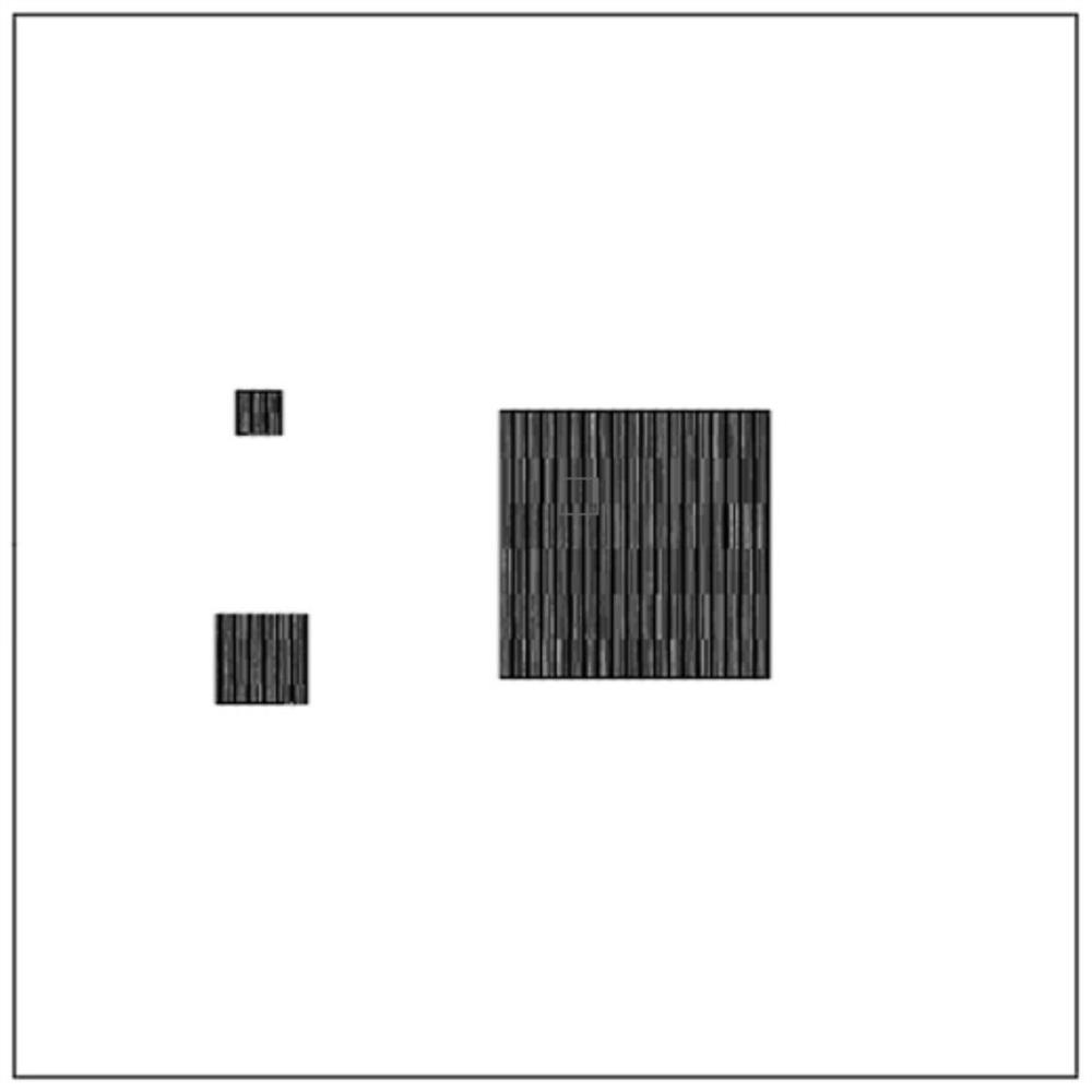
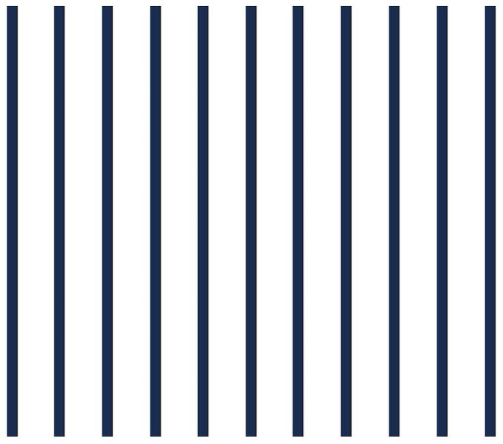
[0049] 1) Spin-coat a layer of HDMS on the silicon wafer substrate first, the solution dosage is 1ml, then spin-coat a layer of AZP4620 photoresist with a thickness of 8 μm, and then use a mask plate with a grid light-transmitting array for exposure. Among them, the width of the light-transmitting area of ​​the mask with a grid light-transmitting array is 10 μm, and the distance between two adjacent grids is 40 μm. The shape and pattern distribution of the mask are as follows: figure 1 As shown, the details of the graphics area are as follows figure 2 As shown, the shaded part is the light-transmitting region.

[0050] 2) Put the structure obtained after exposure in step 1) into a developing solution for development. After development, the area not exposed to light due to the mask plate remains, and the exposed part is washed away. Finally, a photoresist is obtained. A silicon wafer substrate wi...


PUM

PropertyMeasurementUnit
Widthaaaaaaaaaa
Widthaaaaaaaaaa
Wall thicknessaaaaaaaaaa

Abstract

The invention discloses a preparation method of a super-hydrophobic surface with a multi-scale structure. The preparation method comprises the steps of firstly, manufacturing a micron-scale grid pattern on a silicon substrate by using a thick photoresist photoetching method, and manufacturing a groove array on the silicon substrate by using the photoetching grid pattern by using an etching method;then, manufacturing a smaller nano-scale groove array on the groove array through the laser ultra-light micro machining technology; and then using the silicon substrate with the micro-nano structureas a mold, and manufacturing the FEP structure through mold turnover by using a hot stamping method. The FEP structure prepared by the invention is manufactured by taking the silicon substrate with amicro-nano structure as a mold through mold turnover; the super-hydrophobic surface has a corresponding multi-scale structure as shown in an attached drawing, shows super-hydrophobicity in application, and can maintain C-B state stability for a longer time compared with a super-hydrophobic surface of a common microstructure, so that the super-hydrophobic performance is maintained for a long time,and the functions of drag reduction, self-cleaning and the like are shown.

Description

technical field [0001] The invention belongs to the technical field of micro-nano manufacturing, and in particular relates to a method for preparing a micro-nano multi-scale structure superhydrophobic performance surface. Background technique [0002] Due to the potential applications of superhydrophobic structures in surface cleaning, microfluidic systems and biocompatibility, it has become one of the research hotspots in recent years. The superhydrophobic principle of the so-called superhydrophobic structure is mainly to make the liquid in the Cassie-Baxter state on the surface of the microstructure. The angle is very small, and the droplets are easy to roll off the surface, so it has the functions of self-cleaning and drag reduction. However, in a complex water environment, the C-B state is easily destroyed, losing the superhydrophobicity and functions of the surface itself. Contents of the invention [0003] The purpose of the present invention is to provide a method...

Claims


Application Information

Patent Timeline
IPC IPC(8): B81C1/00G03F7/00G03F7/20B82Y40/00
CPCB81C1/00206B81C1/0046G03F7/20G03F7/0002B82Y40/00
Inventor 王朝晖李园郑腾飞
Owner XI AN JIAOTONG UNIV
Why Eureka
Try Eureka