


Quick Research
Generate reliable direction feasibility study reports for your R&D in just a few steps.

Technical Q&A
Discover and master advanced knowledge NOW. Basics, ideas, possibilities, all at once.

Find Solutions
As an expert in R&D theories, this can generate solutions to your technical problems instantly.

Evaluate Feasibility
Analyze your overall solution with one click, know your potential R&D risks in advance.

Monitor Landscape
Get weekly tech updates, stay abreast of the latest tech innovations and key insights.
Zinc oxide-based light-emitting diode and manufacturing method thereof
A light-emitting diode, zinc oxide-based technology, applied in the direction of electrical components, circuits, semiconductor devices, etc., can solve the problems of limiting the ultraviolet luminescence performance of zinc oxide, the influence of device luminous intensity, etc., to achieve mass production, low cost, and high luminous intensity enhanced effect
- Summary
- Abstract
- Description
- Claims
- Application Information
AI Technical Summary
Problems solved by technology
Method used
Image

Examples
Embodiment 1
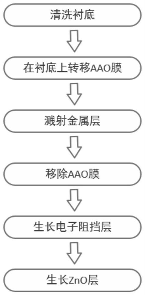
[0033] Such as figure 1 As shown, the present embodiment provides a method for manufacturing a ZnO-based light-emitting diode, including:
[0034] S1: From top to bottom, select 2-inch P-type silicon as the substrate, use acetone and isopropanol to sonicate for 3 minutes, and blow dry with an air gun. An AAO film with a pore size of 20 nm and a pitch of 50 nm was transferred onto the substrate.
[0035] S2: A layer of Ag is grown on the AAO film by magnetron sputtering, the sputtering power is 50W, and the thickness is 20nm.
[0036] S3: The AAO film was removed using Kapton tape, leaving the Ag nanoparticles.
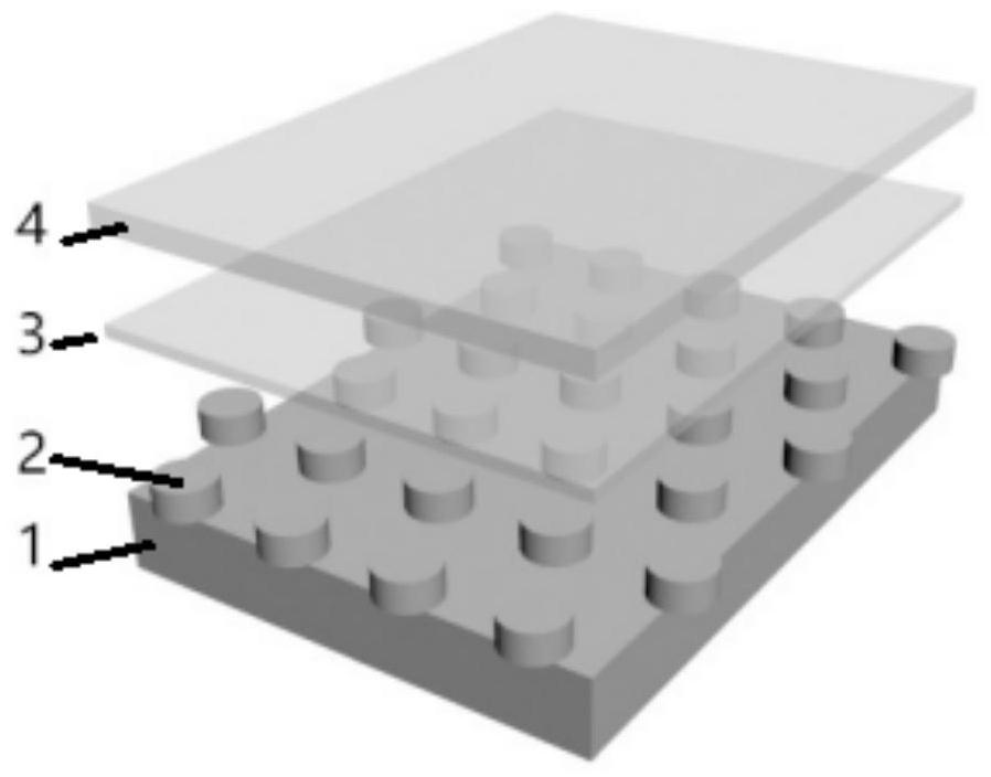
[0037] S4: Growth of Al on nanoparticles by atomic layer deposition (ALD) at 100 °C 2 o 3 The barrier layer was grown to a thickness of 20nm. A ZnO layer was grown on the Al2O3 barrier layer in the same manner to a thickness of 50nm. At this time, the basic structure of the device is completed, and the structure diagram is as follows: figure 2 shown.
[0038] ...
Embodiment 2
[0040] This embodiment provides a method for manufacturing a ZnO-based light-emitting diode, and the specific steps are as in Embodiment 1, including:
[0041] S1: From top to bottom, select 2-inch P-type silicon as the substrate, use acetone and isopropanol to sonicate for 3 minutes, and blow dry with an air gun.
[0042] S2: transfer the AAO film with a pore size of 50 nm and a pitch of 120 nm onto a substrate. A layer of Au was grown on the AAO film by magnetron sputtering, the sputtering power was 100W, and the thickness was 100nm.
[0043] S3: The AAO film was removed using Kapton tape, leaving the Au nanoparticles.
[0044] S4: Growth of Al on nanoparticles by atomic layer deposition (ALD) at 150 °C 2 o 3 The barrier layer was grown to a thickness of 50nm. In the same way at Al 2 o 3 A ZnO layer was grown on the barrier layer with a thickness of 150 nm. At this point the basic structure of the device is complete.
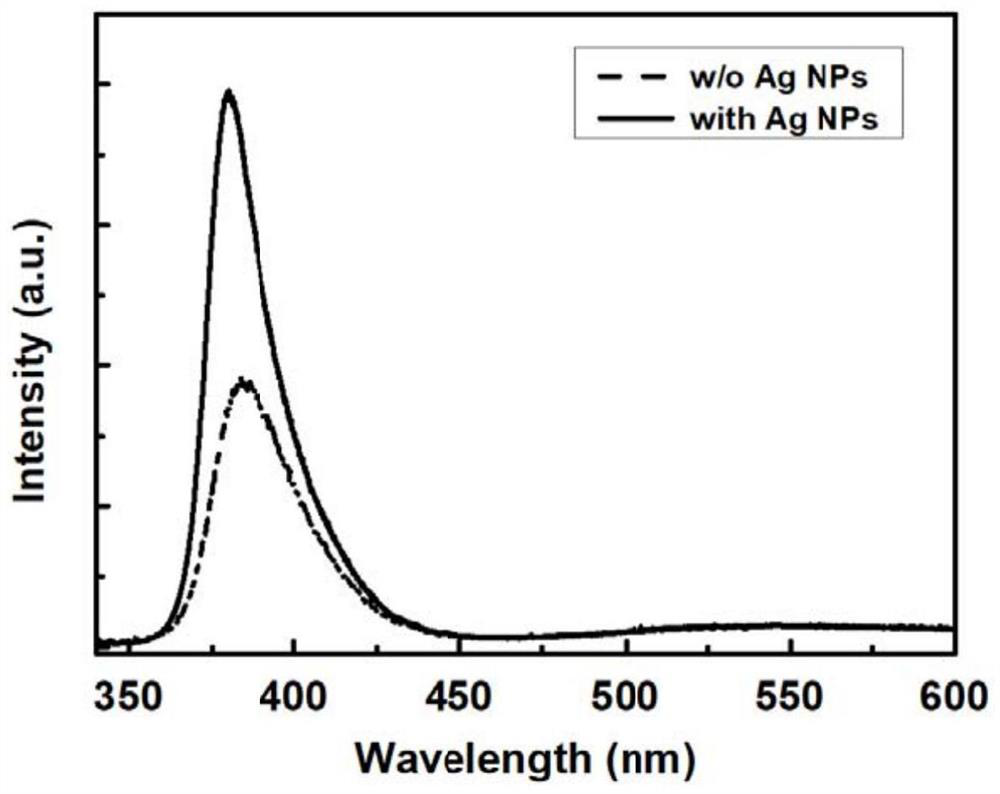
[0045] Compared with ZnO without metal particles...
Embodiment 3
[0047] This embodiment provides a method for manufacturing a ZnO-based light-emitting diode, and the specific steps are as in Embodiment 1, including:
[0048] S1: From top to bottom, select 2-inch P-type silicon as the substrate, use acetone and isopropanol to sonicate for 3 minutes, and blow dry with an air gun.
[0049]S2: Transfer the AAO film with a pore diameter of 100 nm and a pitch of 180 nm to a substrate. A layer of Pt was grown on the AAO film with a thickness of 150 nm using a hydrothermal method.
[0050] S3: The AAO film was removed using Kapton tape, leaving the Pt nanoparticles.
[0051] S4: Growth of Al on nanoparticles by magnetron sputtering at room temperature 2 o 3 The barrier layer was grown with a sputtering power of 200W and a thickness of 100nm. In the same way at Al 2 o 3 A ZnO layer is grown on the barrier layer with a thickness of 300 nm. At this time, the basic structure of the device is completed, and the structure diagram is as follows: ...
PUM
| Property | Measurement | Unit |
|---|---|---|
| Size diameter | aaaaa | aaaaa |
| Spacing | aaaaa | aaaaa |
| Thickness | aaaaa | aaaaa |
Abstract
Description
Claims
Application Information
 - R&D Engineer
- R&D Manager
- IP Professional
- Industry Leading Data Capabilities
- Powerful AI technology
- Patent DNA Extraction
Browse by: Latest US Patents, China's latest patents, Technical Efficacy Thesaurus, Application Domain, Technology Topic, Popular Technical Reports.
© 2024 PatSnap. All rights reserved.Legal|Privacy policy|Modern Slavery Act Transparency Statement|Sitemap|About US| Contact US: help@patsnap.com