NixSiy/Ga2O3 Schottky diode compatible with Si process and preparation method of NixSiy/Ga2O3 Schottky diode

A Schottky diode and process technology, which is applied in semiconductor/solid-state device manufacturing, electrical components, circuits, etc., can solve the problems of small adjustable range of barrier height, high barrier height, and high conduction voltage

Active Publication Date: 2020-10-27
FUDAN UNIV
View PDF11 Cites 0 Cited by
  • Summary
  • Abstract
  • Description
  • Claims
  • Application Information

AI Technical Summary

Problems solved by technology

As a compound semiconductor process, Ga 2 o 3 Schottky diode power devices only use metal electrodes with different work functions to contact the semiconductor surface to form the anode and cathode of the device. In the manufacture of Schottky anodes, the Schottky barrier is fixed due to the fixed work function of the metal. value, so the adjustment of the fine process has limited improvement on the performance of the Schottky diode
At the same time, Ga 2 o 3 The Schottky anode has the disadvantages of high barrier height, small adjustable range of barrier height and high turn-on voltage
[0003] At present, the silicon-based integrated circuit process is the most mature and complex semiconductor manufacturing technology. If some advantages of the silicon-based integrated circuit process can be applied to the compound process, the new structure of the wide-bandgap semiconductor device can be reconstructed and the performance of the device can be improved. , this will be a very innovative research work, but if polysilicon compatible with the silicon process is used as the Schottky electrode, the resistivity will be greatly improved

Method used


Image

  • NixSiy/Ga2O3 Schottky diode compatible with Si process and preparation method of NixSiy/Ga2O3 Schottky diode
  • NixSiy/Ga2O3 Schottky diode compatible with Si process and preparation method of NixSiy/Ga2O3 Schottky diode
  • NixSiy/Ga2O3 Schottky diode compatible with Si process and preparation method of NixSiy/Ga2O3 Schottky diode

Examples


Embodiment 1

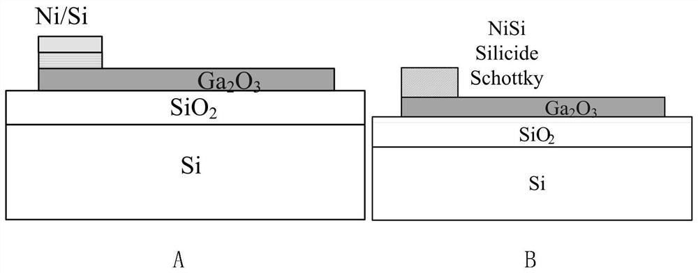
[0036] A Ni that is compatible with the Si process x Si y / Ga 2 o 3 Schottky diode manufacturing method, comprising the following steps:

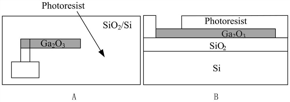
[0037] Step one, the Ga 2 o 3 The film is covered on the working surface of the marking sheet, and the working surface is completely coated with glue.

[0038] In this embodiment, the specific operation of step 1 is as follows:

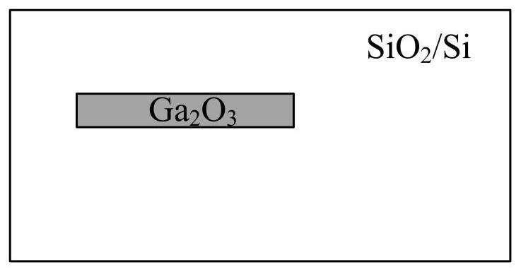
[0039] Choose SiO2 2 / Si double-layer marking sheet is used as the marking sheet of this embodiment, and its SiO 2 The surface serves as a working surface having first and second regions adjoining each other and a third region adjoining and cooperating with the first region.

[0040] Will be from Ga 2 o 3 The area torn off from the single crystal is 3×20μm 2 Ga 2 o 3 Film mechanically transferred to an area of ​​1 × 1 cm 2 SiO 2 SiO / Si double-layer marker sheet 2 surface, with SiO 2 / Si bilayer marker sheet as Ga 2 o 3 For the supporting body of the film, apply glue evenly on the working surface,...


PUM

PropertyMeasurementUnit
thicknessaaaaaaaaaa
thicknessaaaaaaaaaa
thicknessaaaaaaaaaa

Abstract

The invention provides a NixSiy/Ga2O3 Schottky diode compatible with a Si process and a preparation method of the NixSiy/Ga2O3 Schottky diode. The method is used for forming a Schottky electrode and an ohmic electrode on a marking sheet, wherein the working surface of the marking sheet is provided with a first region, a second region and a third region. The method comprises the steps of covering the first region with a Ga2O3 film, and then completely gluing the surface and the working surface of the Ga2O3 film; removing glue on the surface and the working surface of the Ga2O3 film by means ofphotoetching to obtain an anode window; sputtering and depositing Si and Ni at the anode window; rapidly annealing the marking sheet with the glue being removed in an inert atmosphere at a predetermined temperature for a predetermined time; and manufacturing ohmic electrodes with Ga2O3 in the first region and the third region so as to obtain the NixSiy/Ga2O3 Schottky diode. The NixSiy/Ga2O3 Schottky electrode prepared by the method provided by the invention has relatively low resistivity and excellent thermal stability, can be used for preparing a NixSiy/Ga2O3 Schottky anode with adjustable barrier height under the condition of meeting the compatibility with a silicon process, and has a wide application prospect.

Description

technical field [0001] The invention relates to the field of ultra-wide bandgap compound semiconductor technology and the field of Schottky power diodes, in particular to a Ni x Si y / Ga 2 o 3 Schottky diodes and methods of making them. Background technique [0002] In recent years, ultra-wide bandgap semiconductor power devices have attracted more and more attention due to their high energy conversion efficiency and large breakdown voltage. And because the Schottky diode has high switching frequency, small forward voltage drop, and no reverse recovery time, it can be used in high-frequency and high-power conversion. by Ga 2 o 3 material made of Ga 2 o 3 Schottky diode power devices have a bright application potential due to their low conduction loss and switching loss in high voltage and high temperature environments. However, most of the reported Ga 2 o 3 Schottky diode power devices use metal electrodes, in Ga 2 o 3 The surface forms a metal / semiconductor Sch...

Claims


Application Information

Patent Timeline
Patent Type & Authority Applications(China)
IPC IPC(8): H01L29/872H01L21/34
CPCH01L29/66007H01L29/872
Inventor 张卫李晓茜陈金鑫卢红亮黄伟
Owner FUDAN UNIV
Why Eureka
Try Eureka