

Solar cell and preparation method thereof
A technology of solar cells and regions, applied in the field of solar cells, can solve problems such as high short-circuit current of high-efficiency cells
- Summary
- Abstract
- Description
- Claims
- Application Information
AI Technical Summary
Problems solved by technology
Method used
Image

Examples
preparation example Construction
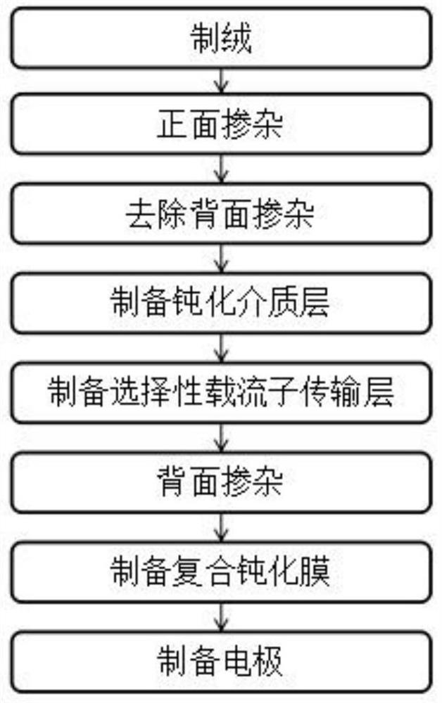
[0063] The invention also discloses a method for preparing a solar cell, such as figure 2 shown, including the following steps:
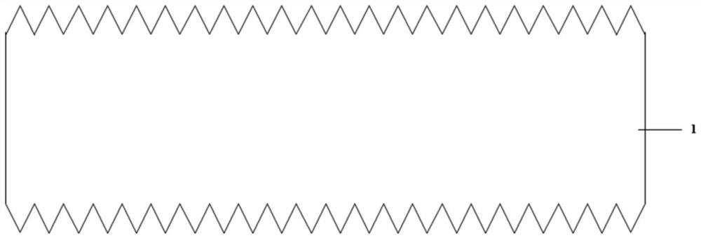
[0064] S1. Provide a p-type or n-type silicon substrate 1 with a resistivity of 0.1-20Ω·cm, and use NaOH or KOH to texture the silicon substrate 1. The structure after texture is as follows image 3 As shown, HCl, O 3 、H 2 o 2 , HF, KOH and other mixed solutions for surface cleaning.
[0065] S2, front doping: use gaseous BCl on the texturing surface of the front of the silicon substrate 1 3 or BBr 3 The source carries out boron diffusion at 700~1100℃ or adopts pH 3 , red phosphorus or B 2 h 6 The ion implantation of the plasma source is followed by annealing at 700-1100°C for doping; the structure after front doping is as follows Figure 4 As shown, a doped layer 2 is formed on the textured surface of the front side of the silicon substrate 1 , silica glass is formed on the top of the doped layer 2 , and a diffusion layer is formed on the...
Embodiment 1
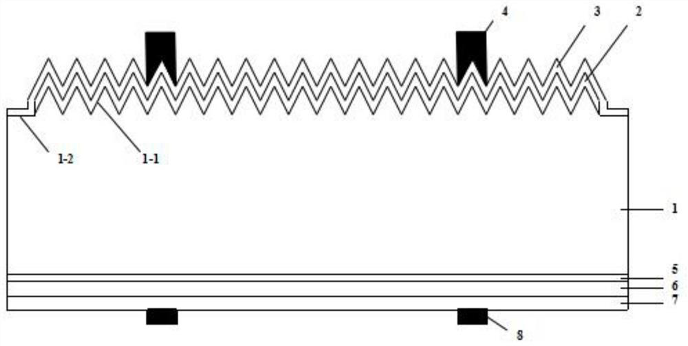
[0095] This embodiment discloses a solar cell and its preparation method. The structure of the solar cell in this embodiment is as follows figure 1 shown.
[0096] In the preparation method of this embodiment, the silicon substrate 1 is an n-type silicon wafer, the front doping is boron diffusion, and the furnace tube is oxidized to prepare silicon dioxide (SiO 2 ) passivation medium layer 5, the selective carrier transport layer 6 is intrinsic intrinsic polysilicon, the selective carrier transport layer 6 is implanted with P by ion implantation to achieve doping, the flow chart of the whole preparation method is as follows figure 2 shown. Specific steps are as follows:
[0097] Front-side doping: select an n-type single crystal silicon wafer with a resistivity of 0.1-20Ω·cm, and place it in a texture-making tank for surface texturing to form a textured structure, such as image 3 Shown; Then the silicon wafer after the texturing is placed in the boron (B) diffusion furnac...
Embodiment 2
[0108] This embodiment discloses a solar cell and its preparation method. The structure of the solar cell in this embodiment is the same as that in Embodiment 1. The difference is that in the preparation method of this embodiment, the chemical method of nitric acid oxidation is used to prepare silicon dioxide (SiO 2 ), the passivation medium layer 5, and the selective carrier transport layer 6 are laminated silicon thin films of P-doped amorphous silicon and intrinsic polysilicon. Specific steps are as follows:
[0109] Front-side doping: select an n-type single crystal silicon wafer with a resistivity of 0.1-20Ω·cm, and place it in a texture-making tank for surface texturing to form a textured structure, such as image 3 Shown; Then the silicon wafer after the texturing is placed in the boron (B) diffusion furnace tube to prepare the p+ doped layer 2, and borosilicate glass is formed on the front side simultaneously, as Figure 4 shown.
[0110] Removal of doping on the ba...
PUM
| Property | Measurement | Unit |
|---|---|---|
| Thickness | aaaaa | aaaaa |
| Resistivity | aaaaa | aaaaa |
| Thickness | aaaaa | aaaaa |
Abstract
Description
Claims
Application Information