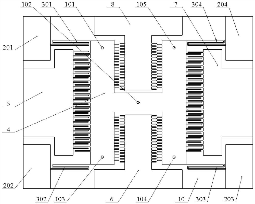
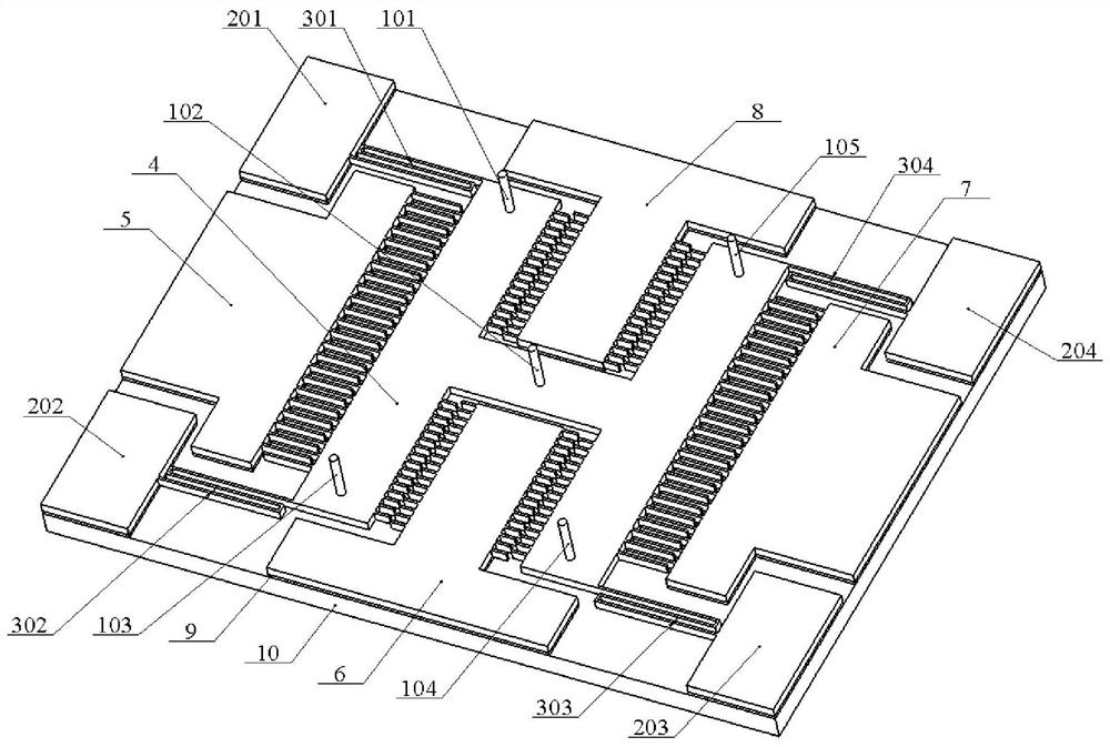
Bionic cilium microsensor based on bistable potential energy adjustment and preparation method of bionic cilium microsensor
A bistable, flow rate sensor technology, applied in the micro-electromechanical field, can solve the problems of sensitivity to environmental temperature changes, low magnification, inability to respond to signal and noise separation, etc., and achieve good zero drift, increased sensitivity, and improved measurement resolution. Effect
- Summary
- Abstract
- Description
- Claims
- Application Information
AI Technical Summary
Problems solved by technology
Method used
Image
Examples
Embodiment 1
[0063] This embodiment provides a method for preparing a bionic cilia flow rate flow direction MEMS sensor, which is manufactured by MEMS microfabrication technology, and the process flow is as follows Figure 4 As shown, the specific process operation is as follows:
[0064] (1) Prepare a double-throw conductive SOI sheet as a substrate, in RNH 3 ·H 2 O:H 2 o 2 :H 2 Soak in a solution of O=1:1:5 at 110°C for 15 minutes, then clean;
[0065] (2) Remove the oxide layer film on the back of the SOI sheet (such as the oxide layer on the back silicon surface), use HF:H 2 O=1:10 Prepare the solution, put the tablet in for about 10 minutes, take out the water, rinse it and dry it;
[0066] (3) Spin-coat HJ6030 positive resist with a thickness of about 6um on the device layer, after drying, use a photolithography machine to expose for about 45 seconds, and obtain a pattern after development;
[0067] (4) Use the SPTS deep silicon etching system to etch the back silicon 300um fo...
Embodiment 2
[0076] The present invention also provides another preparation method for preparing the above-mentioned bionic cilia flow rate MEMS sensor, the device is manufactured by MEMS technology, and the process flow is as follows Figure 5 As shown, the specific process operation is as follows:
[0077] (1) Prepare a double-throw conductive SOI sheet as a substrate, in RNH 3 ·H 2 O:H 2 o 2 :H 2 Soak in a solution of O=1:1:5 at 110°C for 15 minutes, then clean;
[0078] (2) sputtering Cr / Au on the upper surface of the silicon on the SOI sheet device layer;
[0079] (3) Spin-coat HJ6030 positive resist with a thickness of about 6um, after drying, use a photolithography machine to expose for about 45 seconds, and obtain graphics after development;
[0080] (4) Obtain the lead electrode pattern with ion beam etching, and then remove the glue;
[0081] (5) Spin-coat the photoresist again and expose and develop it to obtain a pattern. Use DRIE to etch Si about 60um, which takes about...
PUM
 Abstract
Description
Claims
Application Information


