Silicon-based semiconductor pn junction structure and its preparation method, photocathode and application

A semiconductor and PN junction technology, which is applied in the field of silicon-based semiconductor PN junction structure and its preparation, can solve the problems of complex preparation process and high cost of PN junction, and achieve the effect of improving separation efficiency, excellent stability and strong controllability

Active Publication Date: 2022-02-18
TIANJIN UNIV
View PDF9 Cites 0 Cited by
  • Summary
  • Abstract
  • Description
  • Claims
  • Application Information

AI Technical Summary

Problems solved by technology

[0004] The present invention aims to solve the technical problems of high cost and complicated preparation process for forming a PN junction by heavy doping on the surface of the existing single crystal silicon electrode, and provides a highly efficient and stable silicon-based semiconductor PN junction structure and its preparation method, and On this basis, a silicon-based semiconductor PN junction photocathode and its application are provided

Method used


Image

  • Silicon-based semiconductor pn junction structure and its preparation method, photocathode and application
  • Silicon-based semiconductor pn junction structure and its preparation method, photocathode and application
  • Silicon-based semiconductor pn junction structure and its preparation method, photocathode and application

Examples


Embodiment 1

[0035] (1) Silicon wafer cleaning

[0036] Place the p-Si single crystal (100) silicon chip in the HF solution with a volume concentration of 1% and soak for 15s, rinse it with deionized water, N 2 Blow dry; this step can remove the SiO produced by self-oxidation on the surface of p-Si single crystal (100) silicon wafer 2 ;

[0037] (2)TiO 2 Preparation of anatase nanolayers

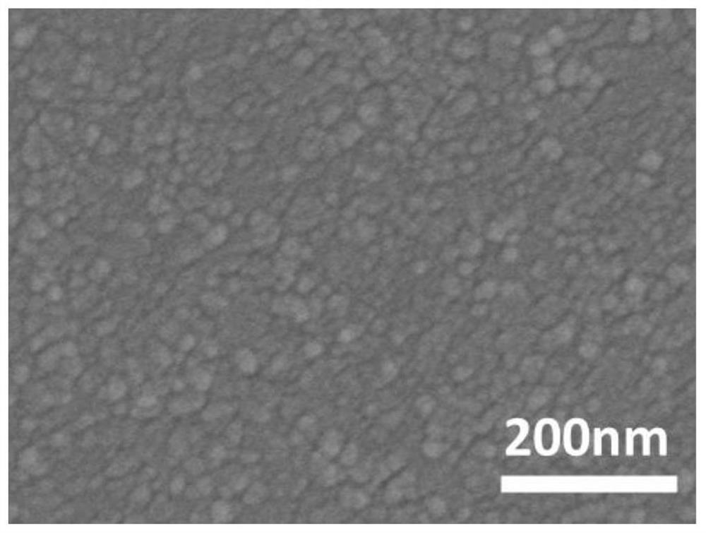
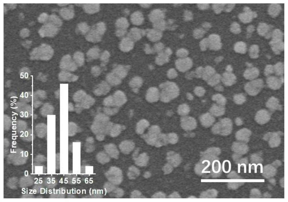
[0038] Will N 2 The blow-dried p-Si single crystal (100) silicon wafer is placed in the chamber of the atomic layer deposition system for deposition. The precursors are tetraisopropyl titanate and water to achieve the deposition of TiO on the surface of the p-type silicon substrate. 2 Nanocrystalline layer; the deposition temperature of atomic layer deposition is 270 ° C, the number of atomic layer deposition cycles is 850, TiO2 The nanocrystalline layer was deposited with a thickness of 26 nm.

[0039] (3) TiO 2 Anatase Nanolayer Reduction

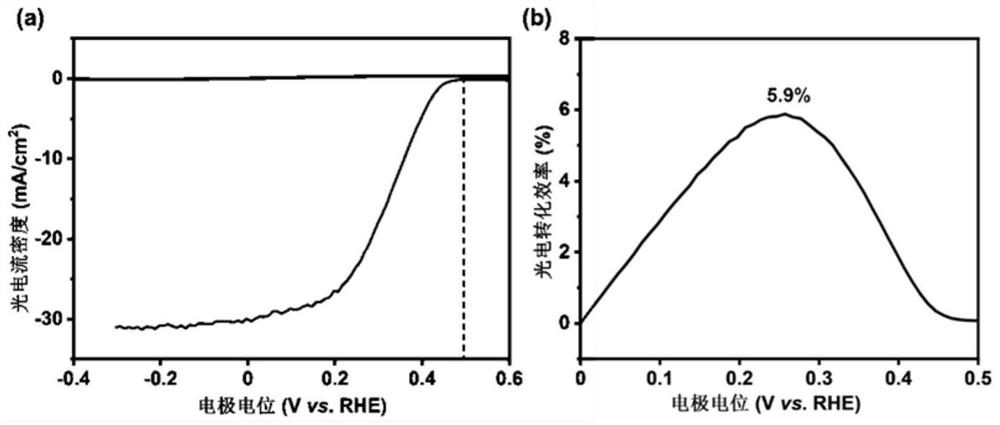
[0040] The encapsulated p-Si / TiO 2 The heterojunction ...

Embodiment 2

[0047] Carry out preparation and reaction with embodiment 1 method, its difference is only that in step (2) atomic layer deposition cycle number is 350, TiO 2 The thickness of the nanocrystalline layer is 10nm.

Embodiment 3

[0049] Carry out preparation and reaction with embodiment 1 method, its difference is only in step (2) in atomic layer deposition cycle number 1200,, TiO 2 The thickness of the nanocrystalline layer is 36nm.


PUM

PropertyMeasurementUnit
thicknessaaaaaaaaaa
thicknessaaaaaaaaaa
thicknessaaaaaaaaaa

Abstract

The invention belongs to the technical field of semiconductor electrodes, and discloses a silicon-based semiconductor PN junction structure, a preparation method, a photocathode and applications thereof. TiO is deposited on the surface of a p-type silicon substrate. 2 Nanocrystalline layer, TiO 2 The nanocrystalline layer forms Schottky contact with the p-type silicon substrate after reduction treatment to obtain a p-type silicon-titania heterojunction structure; its crystalline TiO 2 The Pt auxiliary agent loaded on the nano-layer constitutes a silicon-based semiconductor PN junction photocathode, and the photocathode is used in the photoelectrochemical cell for photo-splitting water for hydrogen production. The silicon-based semiconductor PN junction structure of the present invention can generate high photo-generated voltage and has high stability, and at the same time, the preparation method is simple and easy to implement, has strong controllability, and can realize large-scale production; the silicon-based semiconductor PN of the present invention Junction photocathode utilizes n-type TiO 2 The nanocrystalline layer successfully promotes the separation of photogenerated carriers, improves the onset potential of the silicon-based photocathode, and also protects the p-type silicon substrate.

Description

technical field [0001] The invention belongs to the technical field of semiconductor electrodes, and in particular relates to a silicon-based semiconductor PN junction structure and its preparation method and application. Background technique [0002] As one of the most abundant and inexhaustible sources of energy, solar energy is a promising solution to the energy crisis. At present, the use of solar cells to generate electricity, or the use of solar-based photocatalytic water splitting to produce hydrogen are ideal ways to obtain energy in the future, and have broad development and application prospects. In the design of photoelectrodes, semiconductor materials with excellent light-absorbing ability, electron-transporting ability, and high stability and fewer defects are required as substrates to obtain greater photoelectric conversion efficiency. Single crystal silicon material has excellent light absorption ability (wavelength less than 930nm), charge transfer ability (...

Claims


Application Information

Patent Timeline
Patent Type & Authority Patents(China)
IPC IPC(8): H01G9/20B01J21/06B01J23/42
CPCH01G9/2031B01J21/063B01J23/42B01J35/004Y02E10/542Y02P70/50
Inventor 巩金龙李慧敏王拓刘珊珊
Owner TIANJIN UNIV
Why Eureka
Try Eureka