Laser welding-brazing packaging method and device for three-dimensional weld joint
A packaging method, laser melting technology, applied in the direction of tin feeding device, welding equipment, final product manufacturing, etc., can solve the problem of difficult packaging of micro-nano complex structure devices, achieve excellent material and process compatibility, low residual stress, reduce The effect of energy loss
- Summary
- Abstract
- Description
- Claims
- Application Information
AI Technical Summary
Problems solved by technology
Method used
Image
Examples
Embodiment 1
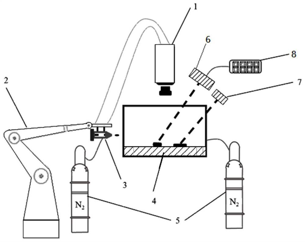
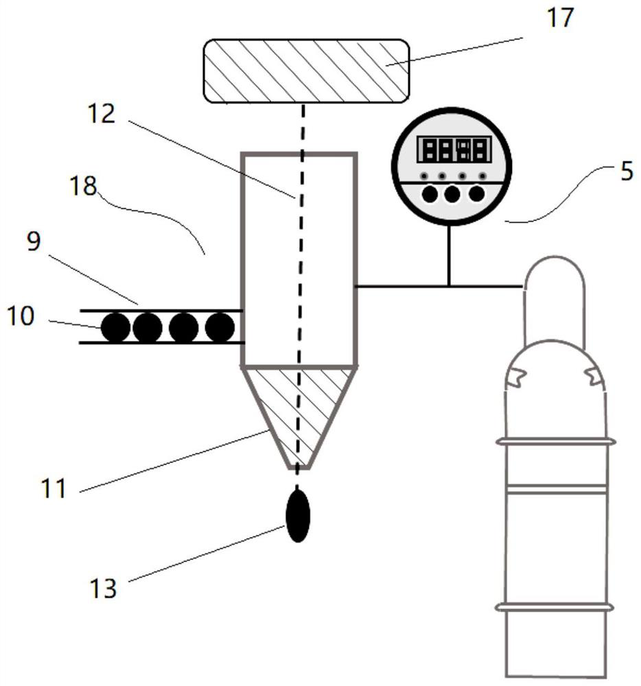
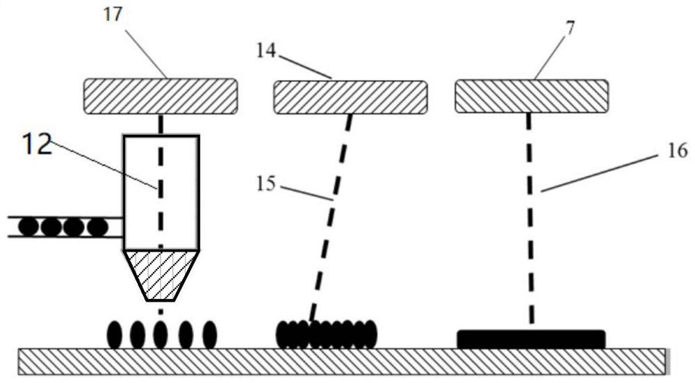
[0045] like Figure 1~Figure 3 As shown, a low-temperature laser melting and brazing packaging device for three-dimensional welding seams, which includes a rotating clamping mechanism 2 for clamping devices to be connected, a solder feeding module 9, a laser melting and brazing module 3, and an auxiliary wetting module 4. The subsequent laser 6 and the post-processing module 7, the laser welding module 3 includes an air jet module 18 and an atmosphere control module 5, the nozzle 11 of the air jet module 18 has a built-in laser 17; the post-processing module 7 It is a low-power continuous laser or a focused infrared heater; the auxiliary wetting module 4 is a heating module, an ultrasonic vibration module, an electrification module or a reducing atmosphere application module, which is integrated on a welding platform for placing devices to be connected; The rotating clamping mechanism 2 includes a rotating and moving drive assembly and a clamping member, the rotating and movin...
Embodiment 2
[0062] like image 3 and Figure 4 Shown, the welding of an aluminum alloy housing and a Kovar alloy sealing cover in a photoelectric signal processor comprises the following steps:
[0063] (1) Pickle the surface of the aluminum alloy and Kovar alloy to be welded to remove pollutants, polish it with a polishing machine to remove oxides, mechanically polish the joint position until the angle between the groove structure and the normal direction is 55°, and the groove depth is 0.3 mm, a 40nm thick Ti layer is plated on the aluminum alloy surface, a 100 nm thick Ni layer is plated on the Kovar alloy surface, and then a 200 nm thick Cr layer is plated;
[0064](2) Prepare Sn52In eutectic solder balls 10 with a diameter of 500 μm, and transport the solder balls 10 to the nozzle 11 through the solder feeding module 9 (ball feeding device);
[0065] (3) Through the built-in laser 17 in the nozzle, the laser 12 is emitted to heat and melt the solder balls, and the melted solder bal...
Embodiment 3
[0070] In an LED device, the Cu pad and the SiC ceramic plate are soldered by preheating the bottom:
[0071] (1) Pickling the Cu pad to be soldered and the surface of the SiC ceramic plate to remove pollutants, polishing with a polishing machine to remove oxides on the surface of the pad, and plating Au / Ni on the Cu pad, the thickness of Au is 100 nm, and the thickness of Ni is 200 nm , a 30 nm thick Ti layer was plated on the surface of the SiC ceramic plate, the angle between the mechanically polished joint position and the groove structure and the normal direction was 45°, and the groove depth was 0.1 mm;
[0072] (2) Preheat the Cu pad and the SiC ceramic plate to be welded to 150 °C, prepare a Sn3.0Ag0.5Cu eutectic solder ball with a diameter of 760 μm, and transport the ball to the nozzle through the ball delivery device;
[0073] (3) Through the built-in laser in the nozzle, the laser is emitted to heat the surface of the solder ball to melt, and the melted solder ball...
PUM
| Property | Measurement | Unit |
|---|---|---|
| particle diameter | aaaaa | aaaaa |
| diameter | aaaaa | aaaaa |
| diameter | aaaaa | aaaaa |
Abstract
Description
Claims
Application Information


