C-axis vertical preferred orientation AlN piezoelectric film and preparation method thereof

A preferred orientation, piezoelectric thin film technology, applied in the manufacture/assembly of piezoelectric/electrostrictive devices, piezoelectric/electrostrictive/magnetostrictive devices, components of piezoelectric devices or electrostrictive devices, etc. Direction, can solve the problems of large film and substrate stress, large film surface roughness, and difficult AlN film, etc., and achieve the effect of small internal stress, continuous and uninterrupted preparation process, and small roughness

Pending Publication Date: 2021-02-19
CHINA ELECTRONICS TECH GRP NO 26 RES INST
View PDF4 Cites 0 Cited by
  • Summary
  • Abstract
  • Description
  • Claims
  • Application Information

AI Technical Summary

Problems solved by technology

Although the traditional magnetron sputtering process can prepare AlN thin films, the horizontal motion energy of the sputtered particles reaching the substrate surface is low, the surface roughness of th...

Method used


Image

  • C-axis vertical preferred orientation AlN piezoelectric film and preparation method thereof
  • C-axis vertical preferred orientation AlN piezoelectric film and preparation method thereof
  • C-axis vertical preferred orientation AlN piezoelectric film and preparation method thereof

Examples


Embodiment Construction

[0033] The following will clearly and completely describe the technical solutions in the embodiments of the present invention with reference to the accompanying drawings in the embodiments of the present invention. Obviously, the described embodiments are only some, not all, embodiments of the present invention. Based on the embodiments of the present invention, all other embodiments obtained by persons of ordinary skill in the art without making creative efforts belong to the protection scope of the present invention.

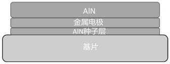
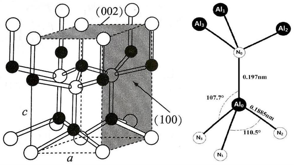
[0034] like Figure 1-2 As shown, a C-axis vertical preferential orientation AlN piezoelectric thin film includes a substrate and an AlN thin film layer, and an AlN seed thin film layer and a metal electrode thin film layer are arranged between the substrate and the AlN thin film layer. The sequence of each film layer includes: from the bottom to the top from the substrate: an AlN seed film layer, a metal electrode film layer and an AlN film layer.

[0035] T...


PUM


Abstract

The invention relates to the technical field of thin film material preparation, in particular to a C-axis vertical preferred orientation AlN piezoelectric thin film and a preparation method thereof, and the preparation method comprises the step: a self-buffer layer AlN thin film, a metal electrode layer and an AlN piezoelectric thin film are sequentially prepared on a sapphire or YAG crystal. Andthe self-buffer layer AlN film induces the orientation of the metal electrode layer, so that the highly C-axis preferred orientation AlN film is prepared on the electrode layer. The sapphire or YAG crystal and the high-purity sputtering target form an angle of 45 degrees, so that the energy of migration motion parallel to the surface of the substrate after sputtering atomic groups reach the substrate is effectively regulated and controlled, the growth of a buffer layer and the C-axis preferred orientation growth of the AlN piezoelectric film are facilitated, and the piezoelectric response andelectromechanical coupling coefficient of the film are improved. According to the method disclosed by the invention, the C-axis preferred orientation AlN film can be grown by utilizing a magnetron sputtering technology at a relatively low temperature, and the obtained AlN film is high in crystallinity and has a relatively high piezoelectric response coefficient and a relatively high electromechanical coupling coefficient.

Description

technical field [0001] The invention relates to the technical field of thin film material preparation, in particular to a C-axis vertical preferred orientation AlN piezoelectric thin film and a preparation method thereof. Background technique [0002] Bulk acoustic wave (BAW) devices are mainly used in radio communication and radar systems, mainly including BAW delay lines, BAW resonators, BAW filters, etc. Among them, thin-film BAW delay lines (BAWDL) have developed rapidly in research and application in recent years. A type of very high frequency device, which has the advantages of small size, light weight, and no edge in the microwave frequency band, and has been widely used in systems such as airborne and missile-borne wireless altimeters. [0003] Traditional BAWDL often uses zinc oxide (ZnO) film, ZnO is an amphoteric oxide, can react with acid and alkali, and is sensitive to ambient humidity, and in the preparation process, the oxygen vacancies of ZnO film are difficu...

Claims


Application Information

Patent Timeline
IPC IPC(8): H01L41/18H01L41/04H01L41/047H01L41/22H01L41/29H01L41/39C23C14/06C23C14/18C23C14/35
CPCC23C14/35C23C14/0617C23C14/18H10N30/80H10N30/87H10N30/85H10N30/01H10N30/06H10N30/093
Inventor 郑泽渔赵雪梅
Owner CHINA ELECTRONICS TECH GRP NO 26 RES INST
Why Eureka
Try Eureka