Silicon carbide single crystal ingot, substrate and preparation method thereof

A silicon carbide substrate and silicon carbide technology, applied in chemical instruments and methods, single crystal growth, single crystal growth, etc., can solve problems such as complex influencing factors, high quality requirements, and incomplete silicon carbide single crystals

Active Publication Date: 2021-04-09
SICC CO LTD
View PDF3 Cites 1 Cited by
  • Summary
  • Abstract
  • Description
  • Claims
  • Application Information

AI Technical Summary

Problems solved by technology

However, the quality requirements for silicon carbide single crystal growth are high, and the influencing factors are complex. The understanding of defects in silicon carbide single crystals is still in an incomplete stage, and the quality of silicon carbide single crystals is important to the manufactured devices and needs to be continuously improved. The quality of SiC substrates to ensure the quality of fabricated devices

Method used


Image

  • Silicon carbide single crystal ingot, substrate and preparation method thereof
  • Silicon carbide single crystal ingot, substrate and preparation method thereof
  • Silicon carbide single crystal ingot, substrate and preparation method thereof

Examples


Embodiment 1

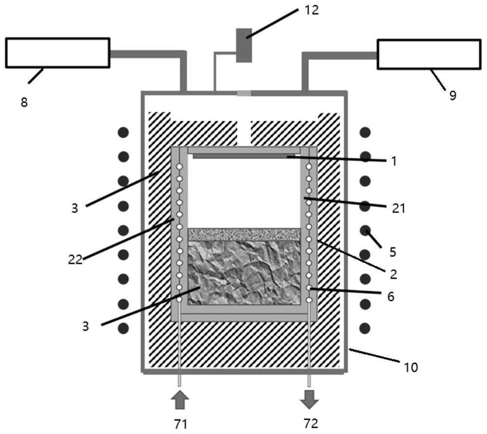
[0075] refer to figure 1 A nitrogen channel 6 is provided on the side wall of the crucible, and the nitrogen channel 6 is arranged in the side wall of the crucible and extends around the inner cavity of the crucible, and the density of the inner side wall of the nitrogen channel is smaller than that of the outer side wall of the nitrogen channel.

[0076] As an embodiment, the crucible 2 includes a liner 21 and a shell 22, and the side wall of the crucible forms a nitrogen channel 6, the nitrogen channel 6 is a spiral channel, and the spiral channel extends helically around the inner cavity of the crucible along the axial direction of the crucible, and the nitrogen channel is at the bottom of the crucible and the top at least once. For example, the nitrogen channel extends from the gas inlet 71 at the bottom of the crucible to the top of the crucible, and then extends to the bottom of the crucible to form a gas outlet 72 .

[0077] Specifically, the inner liner 21 and the out...

Embodiment 2

[0080] refer to figure 1 According to an embodiment of the present application, a method for preparing a silicon carbide single crystal ingot using the crucible of Example 1 comprises the following steps:

[0081] 1) Preparation of silicon carbide single crystal ingot:

[0082] The crucible with the nitrogen channel of embodiment 1 is provided, the nitrogen channel is arranged in the side wall of the crucible and extends around the crucible inner cavity, and the inner side wall of the nitrogen channel is less than the density of the outer side wall of the nitrogen channel;

[0083] Place the silicon carbide seed crystal 1 on the inner top of the crucible 2 and the silicon carbide raw material 3 on the inner bottom of the crucible 2, assemble the heat preservation structure 3 outside the crucible 2, place it in the crystal growth furnace 4, and use the induction coil 5 for heating;

[0084] The temperature controller 12 controls the temperature of the crystal growth furnace, c...

Embodiment 3

[0092] Example 3 Preparation of silicon carbide single crystal ingot 1#

[0093] The preparation method of silicon carbide single crystal ingot 1# comprises the following steps:

[0094] The crucible with the nitrogen channel of embodiment 1 is provided, the nitrogen channel is arranged in the side wall of the crucible and extends around the inner cavity of the crucible, and the density of the inner wall of the nitrogen channel is 1.70g / cm 3 , the density of the shell is 1.90g / cm 3 ;

[0095] Put the silicon carbide seed crystal on the inner top of the crucible and the silicon carbide powder on the inner bottom of the crucible, assemble the heat preservation structure outside the crucible and seal it in the crystal growth furnace;

[0096] Control the temperature and pressure of the crystal growth furnace and the argon flow into the crystal growth furnace to clean and remove impurities in the crystal growth furnace;

[0097] Heating stage: adjust the temperature of the crys...


PUM

PropertyMeasurementUnit
widthaaaaaaaaaa
diameteraaaaaaaaaa
diameteraaaaaaaaaa

Abstract

The invention relates to a silicon carbide single crystal ingot, a substrate and a preparation method thereof, and belongs to the field of semiconductor materials. The silicon carbide substrate contains a nitrogen element, the silicon carbide substrate has no more than 50 hexagonal color spots, and the edges forming the hexagonal color spots are perpendicular to the <10-10> direction. The edges of the hexagonal color spots comprise inner side edges and outer side edges, the inner side edges defines a hexagonal area, cavities are formed between the inner side edges and the outer side edges, and the centers of not smaller than 80% of the cavities are located on one side of the central axis between the inner side edges and the outer side edges. The invention provides the nitrogen-containing silicon carbide substrate with novel defects, namely few hexagonal color spots and cavity defects, the resistivity of the silicon carbide substrate is uniform, and a semiconductor device prepared from the silicon carbide substrate is excellent in electrical performance; and the performance of the silicon carbide substrate such as breakdown field intensity is excellent, and the number of cavities generated by extension of the manufactured device is extremely small.

Description

technical field [0001] The application relates to a silicon carbide single crystal ingot, a substrate and a preparation method thereof, belonging to the field of semiconductor materials. Background technique [0002] Silicon carbide single crystal is one of the most important third-generation semiconductor materials. It is widely used in power electronics, RF devices, optoelectronic devices and other fields. At present, the main preparation method of silicon carbide single crystal is the physical vapor transport (PVT) method, which is also the most successful method for growing large-diameter SiC crystals so far. It mainly transports the gas phase source generated by the sublimation of the silicon carbide raw material at high temperature to the seed crystal to recrystallize and grow SiC crystal. [0003] Currently mature SiC devices include: silicon carbide Schottky diodes, which mainly use junction barrier Schottky diodes or hybrid p-n Schottky diode structures; silicon c...

Claims


Application Information

Patent Timeline
Patent Type & Authority Applications(China)
IPC IPC(8): C30B29/36C30B23/00H01L29/16H01L29/30
CPCC30B29/36C30B23/002H01L29/1608H01L29/30
Inventor 方帅高宇晗高超石志强杨世兴宗艳民
Owner SICC CO LTD
Why Eureka
Try Eureka