
Preparation method of two-dimensional In2S3/SnS heterojunction crystal material

A crystalline and heterogeneous technology, applied in the field of preparation of two-dimensional In2S3/SnS heterogeneous crystalline materials, can solve the problems of complex reaction process, destruction of product structure and properties, complicated synthesis process, etc., to achieve high crystal quality and reduce energy consumption. , the effect of reducing the temperature

Active Publication Date: 2021-04-16
HUAZHONG UNIV OF SCI & TECH
View PDF4 Cites 5 Cited by
  • Summary
  • Abstract
  • Description
  • Claims
  • Application Information

AI Technical Summary

Problems solved by technology

Vapor deposition can be divided into one-step method and two-step or multi-step method (specifically, undergoing multiple vapor deposition processes), but multi-step vapor deposition inevitably makes the synthesis process more complicated. The structural properties of the obtained product may also be destroyed in the second step reaction process
One-step vapor deposition synthesis of heterostructures has also been reported. The sequential formation of heterojunctions can be achieved by changing the composition of the reactive gas environment, but the complex gas environment will inevitably lead to more complex reaction processes.

Method used


Image

  • Preparation method of two-dimensional In2S3/SnS heterojunction crystal material
  • Preparation method of two-dimensional In2S3/SnS heterojunction crystal material
  • Preparation method of two-dimensional In2S3/SnS heterojunction crystal material

Examples


Embodiment 1

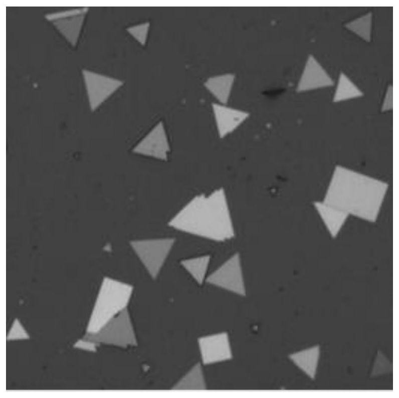
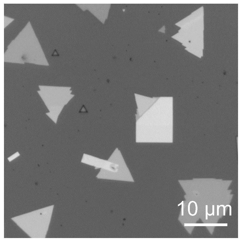
[0030] A horizontal tube furnace with a single temperature zone is used as the reaction device. The tube length of the horizontal tube furnace is 90cm, the outer diameter is 25mm, the tube wall thickness is 2mm, the range of the constant temperature zone is 10cm, and the temperature of the central temperature zone (corresponding to the center of the furnace) is 830°C , the temperature in the downstream deposition area is 600°C, and the heating method is rapid heating (in advance, the tube slide rail furnace is heated to the specified reaction temperature in the non-reaction area, and then the furnace is quickly moved to the reaction area for rapid temperature increase). Using In 2 S 3 and SnS powder (purity>99.99%) as In 2 S 3 and SnS source, adding NaCl at the same time to obtain the precursor (in the precursor, the mass ratio of indium sulfide to tin sulfide is 2:1), and at the same time, the molecular sieve is placed above the precursor and placed in the central temperatu...

Embodiment 2

[0034] A horizontal tube furnace with a single temperature zone is used as the reaction device. The tube length of the horizontal tube furnace is 90cm, the outer diameter is 25mm, the tube wall thickness is 2mm, the range of the constant temperature zone is 10cm, the temperature in the central temperature zone is 820°C, and the temperature in the downstream deposition zone The temperature is 600°C, and the heating method is rapid heating (in advance, the tube slide rail furnace is heated to the specified reaction temperature in the non-reaction area, and then the furnace is quickly moved to the reaction area for rapid temperature increase). Using In 2 S 3 and SnS powder (purity>99.99%) as In 2 S 3 and SnS source, adding NaCl at the same time to obtain a precursor (in the precursor, the mass ratio of indium sulfide to tin sulfide is 2:1), and at the same time, molecular sieves are placed above the precursor and placed in the central temperature zone; A 1cm*1cm piece of fluor...

Embodiment 3

[0036] A horizontal tube furnace with a single temperature zone is used as the reaction device. The tube length of the horizontal tube furnace is 90cm, the outer diameter is 25mm, the tube wall thickness is 2mm, the range of the constant temperature zone is 10cm, the temperature in the central temperature zone is 850°C, and the temperature in the downstream deposition zone The temperature is 600°C, and the heating method is rapid heating (in advance, the tube slide rail furnace is heated to the specified reaction temperature in the non-reaction area, and then the furnace is quickly moved to the reaction area for rapid temperature increase). Using In 2 S 3 and SnS powder (purity>99.99%) as In 2 S 3 and SnS source, adding NaCl at the same time to obtain a precursor (in the precursor, the mass ratio of indium sulfide to tin sulfide is 2:1), and at the same time, molecular sieves are placed above the precursor and placed in the central temperature zone; A 1cm*1cm piece of fluor...


PUM

PropertyMeasurementUnit
thicknessaaaaaaaaaa
thicknessaaaaaaaaaa

Abstract

The invention belongs to the field of nano semiconductor materials, and discloses a preparation method of a two-dimensional In2S3 / SnS heterojunction crystal material. The preparation method comprises the following steps: mixing indium sulfide, stannous sulfide and sodium chloride to obtain a precursor, putting the precursor in a central temperature region of a single-temperature-region reaction furnace, under the condition of introducing a carrier gas, heating the reaction furnace to a preset target temperature to carry out a reaction so as to bring gas-phase In2S3 and gas-phase SnS generated by heating evaporation of the precursor into a deposition region located at the downstream of the central temperature region by using the carrier gas, thereby forming the two-dimensional In2S3 / SnS heterojunction crystal material on a substrate located at the downstream deposition region through deposition. By improving the one-step reaction principle, key reaction conditions and parameters (such as raw material composition, reaction temperature conditions and the like) of the preparation method, compared with the prior art, the two-dimensional in-plane and / or vertical In2S3 / SnS heterojunction can be prepared by a one-step method, and the preparation method is simple in mechanism and convenient to regulate and control.

Description

technical field [0001] The invention belongs to the field of nano-semiconductor materials, and more specifically relates to a two-dimensional In 2 S 3 / SnS heterogeneous crystal material preparation method. Background technique [0002] Two-dimensional heterostructures have attracted considerable attention in recent years due to their unique electrical and optical properties, making them potential candidates for p-n diodes, photodetectors, transistors, sensors as well as light-emitting diodes (Nat.Commun.2015, 6,7311). The heterojunction formed by two-dimensional semiconductors has a wide range of excellent properties, such as tunable band gap (Nano Lett. 2014, 14, 3185), excitonic spectrum and work function (Science 2014, 344, 725). Since the graphene / boron nitride (BN) heterojunction was first reported, 2D transition metal dichalides (TMDs)-MX based 2 Lateral heterostructures of (M=Mo, W; X=S, Se) have attracted increasing attention and have been widely synthesized. ...

Claims


Application Information

Patent Timeline
Patent Type & Authority Applications(China)
IPC IPC(8): C30B29/46C30B23/02
Inventor 周兴左念翟天佑
Owner HUAZHONG UNIV OF SCI & TECH
Learn More