Preparation method of multilayer electronic product

A technology for electronic products and insulating layers, which is applied in the field of preparation of multilayer electronic products, and can solve the problems of inability to achieve integration, low production efficiency, and inability to apply industrially

Active Publication Date: 2021-04-20
广东绿展科技有限公司
View PDF5 Cites 1 Cited by
  • Summary
  • Abstract
  • Description
  • Claims
  • Application Information

AI Technical Summary

Problems solved by technology

However, the single nozzle of electrofluid printing is too large to achieve the integration level like piezoelectric inkjet ...

Method used


Image

  • Preparation method of multilayer electronic product
  • Preparation method of multilayer electronic product
  • Preparation method of multilayer electronic product

Examples


preparation example Construction

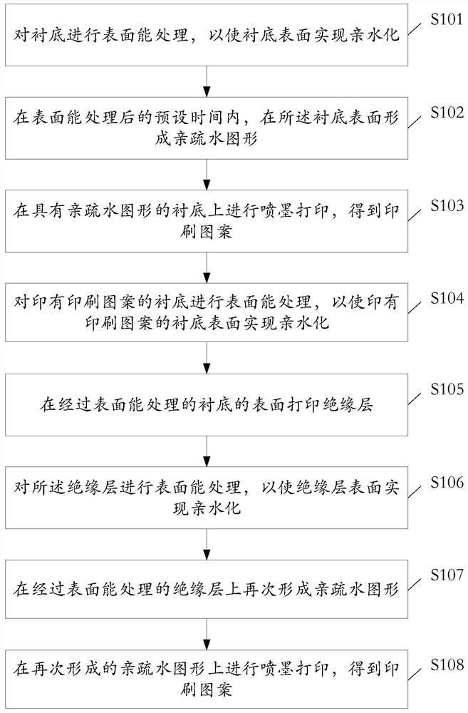
[0065]Such asfigure 1 As shown, the present invention provides a method of preparing a multilayer electronic product, including:

[0066]S101, the substrate can be processed so that the surface of the substrate is hydrophilized;

[0067]The substrate of the present invention needs to be performed in advance, the surface energy treatment is preferably a strong oxidation treatment, and the specific process includes cleaning the substrate; drying the substrate after the cleaning; At least one of the ozone treatment, oxygen or oxidation, ionic treatment, and ultraviolet light treatment, and the Si-O- (H) group of the substrate surface.

[0068]Specifically, when the strong oxidation treatment is ozone treatment, it has the advantages of simple and convenient, high-quality equipment.

[0069]Specifically, when the strong oxidation is treated with an oxygen or oxygen, a vacuum plasma and an atmospheric plasma treatment (generally also referred to as corona treatment). Vacuum plasma needs to evacuate,...

Embodiment 1

[0158](1) The glass is used as a substrate, and the substrate is performed by highly active ozone components produced by the ultraviolet cleaning machine for 5-50 minutes (preferably 30 minutes), so that the surface of the substrate is active Si- O- (h) group;

[0159](2) The seal made of silicone rubber containing the -O-Si-R group is selected from the seal of the polydimethylsiloxane;

[0160](3) In 1s after the end of the strong oxidation treatment, the printed roller of the seal is fixed to the substrate surface of the Si-O- (H) group, and the contact pressure is limited to around 1000Pa. . The roller pressure is 50 mm / s, and the width of 50 microns in accordance with the printing roller and the plane contact region is estimated, the average contact time of the seal and the substrate surface is substantially 1 ms. The water contact angle of the substrate is made from about 15 ° C to about 70 ° C;

[0161]The seal is separated from a substrate with a Si-O- (H) group to obtain a rocket p...

Embodiment 2

[0170](1) The glass is used as a substrate, and the substrate is treated with a spray gun treated with a normal pressure plasma, and the average treatment time is 3-5 s, so that the substrate is formed to form an active Si-O- (H) group;

[0171](2) The seal made of silicone rubber containing the -O-Si-R group is made of methyl vinyl silicone rubber.

[0172](3) In 30s after strong oxidation treatment, the printed roller of the stamp is fixed to the substrate surface of the Si-O- (H) group, and the contact pressure is limited to about 2000 Pa. The roller pressure velocity is 5 mm / s, which is estimated according to the width of the printed roller and the planar contact region, and the average contact time of the seal and the substrate surface is substantially 10 ms, which causes the water contact angle of the substrate from about 20 ° C to About 75 ° C;

[0173]The seal is separated from a substrate with a Si-O- (H) group to obtain a rocket pattern;

[0174](4) The ink containing the conductive...


PUM

PropertyMeasurementUnit
Line widthaaaaaaaaaa
Surface tensionaaaaaaaaaa

Abstract

The invention discloses a preparation method of a multilayer electronic product. The preparation method comprises the following steps: (1) carrying out surface energy treatment on a substrate; (2) forming a hydrophilic and hydrophobic pattern on the surface of the substrate within a preset time after the surface energy treatment; (3) carrying out ink-jet printing on the substrate with the hydrophilic and hydrophobic pattern to obtain a printed pattern; (4) performing surface energy treatment on the substrate printed with the printed pattern; (5) printing an insulating layer on the surface of the substrate subjected to surface energy treatment; (6) performing surface energy treatment on the insulating layer; (7) forming a hydrophilic and hydrophobic pattern on the insulating layer subjected to surface energy treatment again; and (8) carrying out ink-jet printing on the hydrophilic and hydrophobic pattern formed again, and obtaining a printed pattern. By the adoption of the method, large-scale mass production of printing of the multi-layer fine circuit can be achieved, cost is low, industrial application is facilitated, environmental protection and energy conservation are achieved, and subsequent waste liquid treatment procedures are reduced.

Description

Technical field[0001]The present invention relates to the technical field of circuit printing, and more particularly to a method of preparing a multilayer electronic product.Background technique[0002]The integration and low-cost manufacturing of the circuit is the main trend of industrial development. The printing and processing method determines its unique advantages in some electronic products manufacturing, which is expected to have a low integration circuit with its simplified process and low cost. Wide applications are obtained in manufacturing. For example, the screen printing electrode is currently a standard process for the production of photovoltaic cells worldwide, while inkjet printing is mainstream technologies such as flexible OLED film packages.[0003]In the past few decades, an integrated circuit (including board and chip, etc.) mainly reduce standards, including complex photolithography, development, etching, etc., although there is a high resolution and more Good pro...

Claims


Application Information

Patent Timeline
IPC IPC(8): H01L51/00H05K3/12B41M3/00B41M5/00C09D11/36C09D11/38C09D11/52
Inventor 林剑马昌期曾超邢建博
Owner 广东绿展科技有限公司
Why Eureka
Try Eureka